Optical filter

a filter and optical technology, applied in the field of optical filters, can solve the problems of low energy efficiency of a device using a hole-type filter and large amount of light absorption, and achieve the effect of large surface area and greater degree of freedom

Inactive Publication Date: 2010-09-02
CANON KK
View PDF11 Cites 32 Cited by
  • Summary
  • Abstract
  • Description
  • Claims
  • Application Information

AI Technical Summary

Benefits of technology

[0015]The filters described in the above Patent Documents 1 and 2 uses peripheral structures which have apertures or protrusions formed in a metal film having a relatively large surface area with pitches corresponding to wavelengths of the surface plasmons to control the optical properties. That is, the interference between the surface plasmons propagating along the peripheral structures selects the surface plasmon waves with their respective wavelengths corresponding to the pitches, and the selected waves then gather the intensities each other to increase the intensity of a transmitted light and the intensity of a reflected light.
[0079]According to the present invention it is possible to provide a high-transmittance optical filter in which light absorption is less than a hole-type metallic thin film filter in a waveband region containing a visible light region.
[0080]Further, according to the present invention it is possible to provide an optical filter having a greater degree of freedom regarding the selection of size in comparison with filters which utilize the surface plasmon corresponding to the peripheral structure in a metal film having a relatively large surface area.

Problems solved by technology

However, in this kind of hole-type metallic thin film filter, because a large proportion of space is occupied metal, there is a large amount of light absorption.
Consequently, there is the possibility that the energy efficiency of a device that uses a hole-type filter will be low.

Method used


Image

  • Optical filter
  • Optical filter
  • Optical filter

Examples


first embodiment

Single-Layer Optical Filter and Laminated Optical Filter

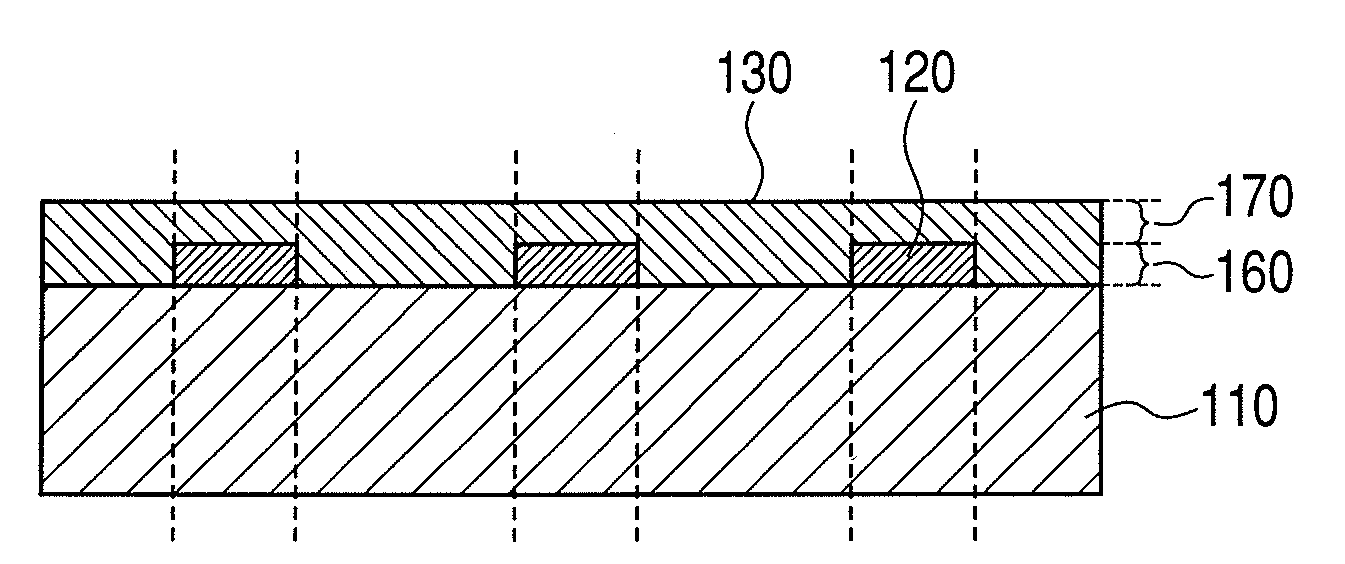
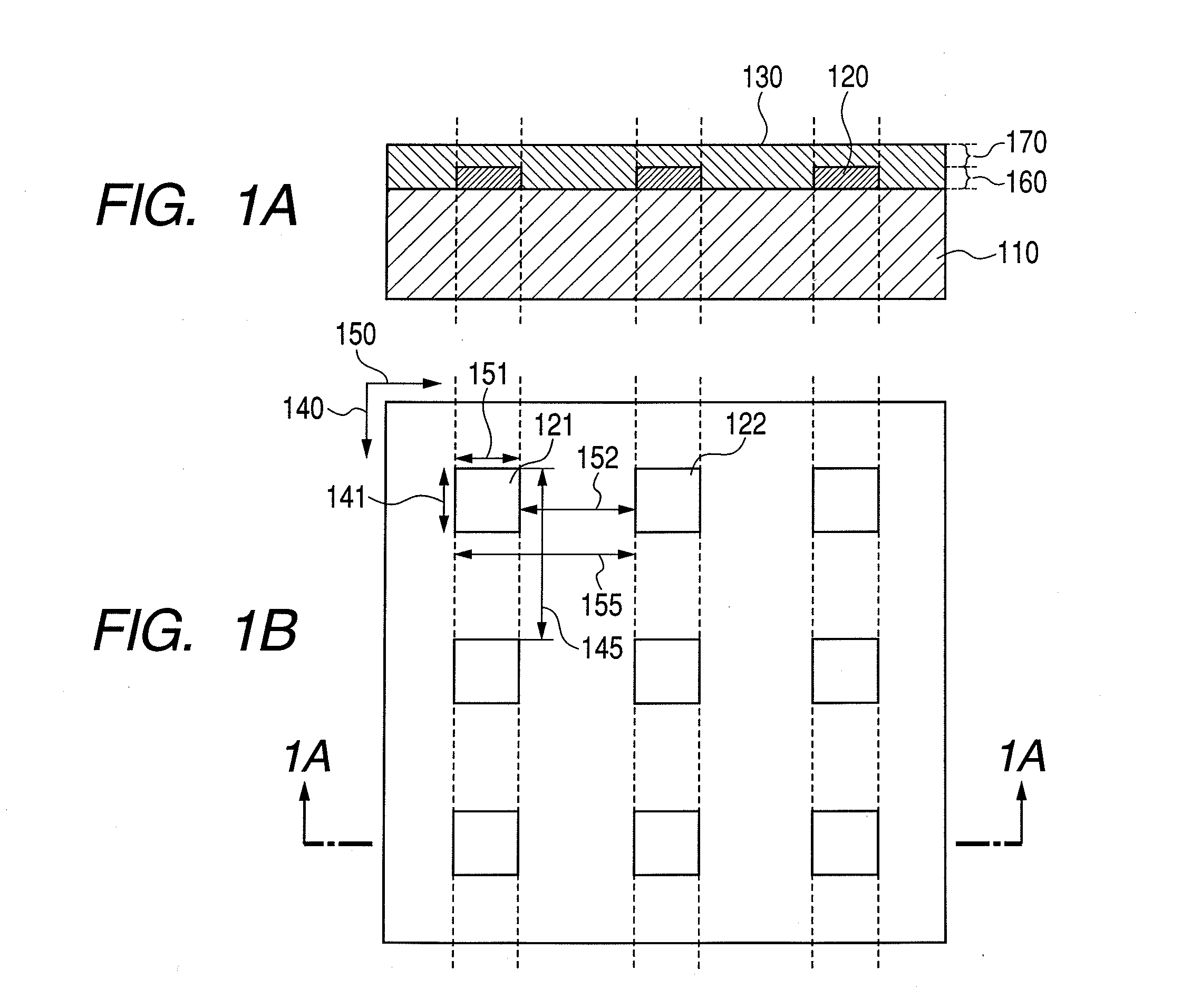
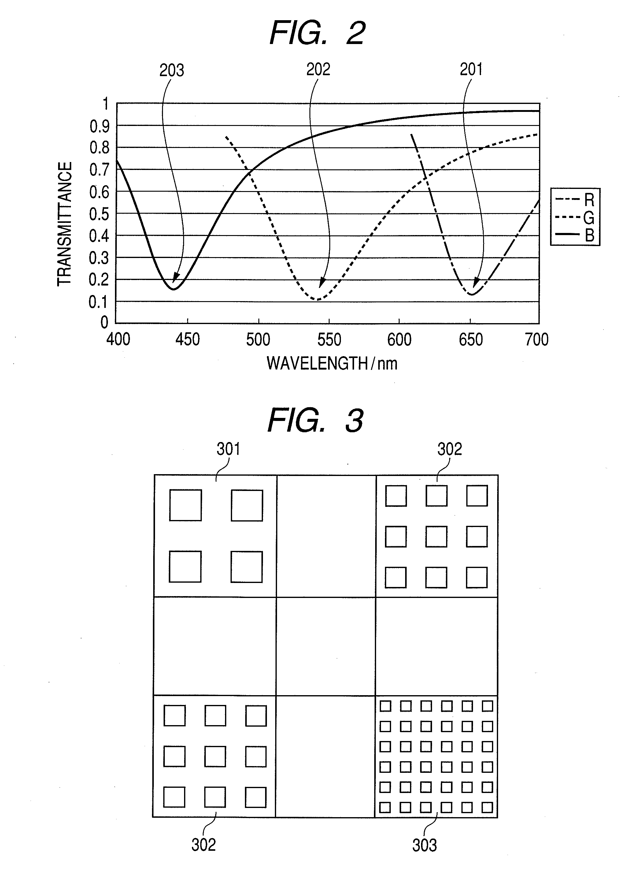
[0126]Hereunder, an embodiment of the present invention is described using the drawings. First, the items denoted by reference numerals in the FIGS. are listed: 110: dielectric substrate, 120: metal structure, 121: first metal structure, 122: first metal structure, 130: dielectric layer, 140: first direction, 141: first length, 145: period, 150: second direction, 151: second length, 155: period, 160: thickness of metal structure, 170: thickness after subtracting metal structure thickness from dielectric layer thickness, 201: transmission spectrum R, 202: transmission spectrum G, 203: transmission spectrum B, 301: region, 302: region, 303: region, 401: first metal structure, 402: first metal structure group, 403: first metal structure, 404: first metal structure group, 405: period, 406: period, 407: first metal structure, 408: second metal structure, 501: first metal structure group, 502: first direction, 503: second direction, ...

second embodiment

Bayer Array

[0196]According to the present embodiment, an RGB filter arranged in a Bayer array is described.

[0197]In FIG. 3, for example, the aforementioned optical filter R (transmission spectrum 201) is arranged in a region 301, the optical filter G (transmission spectrum 202) is arranged in a region 302, and the optical filter B (transmission spectrum 203) is arranged in a region 303. By arranging the optical filters in this manner, it is possible to construct a color filter that is arranged in a Bayer array using the filters according to the present invention.

[0198]The above color filter can be used as a color filter for image capturing device. Region 301 etc. of the color filter has an area corresponding to one pixel, which may be greater than an area covered by the photoelectric conversion device (photoelectric conversion part).

[0199]According to the present embodiment, the sizes of the metal structures and the periods at which the metal structures are arranged differ for each ...

third embodiment

Triangular Lattice

[0204]FIG. 16 is a view that illustrates an embodiment in which metal structures are arranged in a triangular lattice shape. In the case of a triangular lattice arrangement, since the unit vector components of the lattice are not orthogonal, it is possible to reduce the dependence with respect to incident light polarization of the optical characteristics of the filter in comparison to a tetragonal lattice shape arrangement.

[0205]This kind of triangular lattice arrangement can also be expressed as a plurality of metal structure group arranged in a tetragonal lattice shape being disposed in overlapping regions.

[0206]More specifically, it is possible to express this arrangement in terms of a first metal structure group 1602 including first metal structures 1601 and a second metal structure group 1604 including second metal structures 1603 being arranged in overlapping regions.


PUM


Abstract

An optical filter that transmits light of the visible light region includes a dielectric substrate; a dielectric layer that is formed on a surface of the dielectric substrate; and a first metal structure group in which a plurality of first metal structures are arranged two-dimensionally in an isolated state in the in-plane direction of the dielectric substrate, that is provided between the dielectric substrate and the dielectric layer, comprising: the first metal structures having first and second lengths in first and second directions orthogonal to each other, which lengths are equal to or less than a first wavelength in the visible light region; and a transmittance of the first wavelength being reduced or a reflectance being increased by surface plasmons induced on a surface of the first metal structures by resonance between light incident on the dielectric substrate or the dielectric layer and the first metal structures.

Description

TECHNICAL FIELD[0001]The present invention relates to an optical filter that utilizes localized surface plasmon.BACKGROUND ART[0002]Recently, hole-type optical filters in which apertures are periodically arranged in arrays on a metallic thin film and which perform wavelength selection utilizing surface plasmons have been proposed in Patent Document 1 and Non-Patent Document 1.[0003]Conventionally, although also depending on the film thickness, the transmittance of a metallic thin film including an aperture diameter of a size that is less than or equal to a light wavelength is considered to be less than approximately 1%.[0004]However, as described in Patent Document 1, when apertures of a predetermined size are arrayed on a metallic thin film at a period that is consistent with the wavelength of plasmons, the transmittance of light of a wavelength that induces surface plasmons is significantly enhanced.[0005]Further, Non-Patent Document 1 teaches that transmission spectra of RGB can ...

Claims


Application Information

Patent Timeline
Patent Type & Authority Applications(United States)
IPC IPC(8): G02B5/26
CPCG02B5/008G02B5/223G02B5/204G02B5/201H01L27/14621H01L27/1462
Inventor YAMADA, TOMOHIROOGINO, MASAYAINAO, YASUHISA
Owner CANON KK
Why Eureka
Try Eureka