Laser device, laser display apparatus, laser radiating apparatus, and nonlinear optical element

a laser display and laser technology, applied in the direction of laser details, instruments, light demodulation, etc., can solve the problems of low efficiency, limited length of poling structure effective for individual wavelengths, and inability to reduce speckle noise in turn, so as to enhance the efficiency of conversion and reduce the effect of speckle nois

Inactive Publication Date: 2010-09-02
SONY CORP
View PDF6 Cites 23 Cited by
  • Summary
  • Abstract
  • Description
  • Claims
  • Application Information

AI Technical Summary

Benefits of technology

[0013]Since the wavelength width of the semiconductor laser array is as wide as several nanometers, the semiconductor laser array has the effect of reducing the speckle noise described above. However, when the wavelength width of the laser beam is narrowed in order to enhance the efficiency of conversion to the second-order harmonic, the speckle noise can not be reduced in turn.
[0014]In addition, with the technique described in Patent Document 3, the semiconductor laser having the longitudinal multimode, and a plurality of poling structures each corresponding to the fundamental wave are provided, thereby making it

Problems solved by technology

However, when the wavelength width of the laser beam is narrowed in order to enhance the efficiency of conversion to the second-order harmonic, the speckle noise can not be reduced in turn.
Therefore, in this case, the length of the poling structure effective for the individual wavelengths is limited, and as a result, the efficiency becomes very low.
As a result, the device i

Method used


Image

  • Laser device, laser display apparatus, laser radiating apparatus, and nonlinear optical element
  • Laser device, laser display apparatus, laser radiating apparatus, and nonlinear optical element
  • Laser device, laser display apparatus, laser radiating apparatus, and nonlinear optical element

Examples


first embodiment

1. First Embodiment

The First Case where a Poling Period and a Poling Duty Ratio Both Change in a Propagating Direction

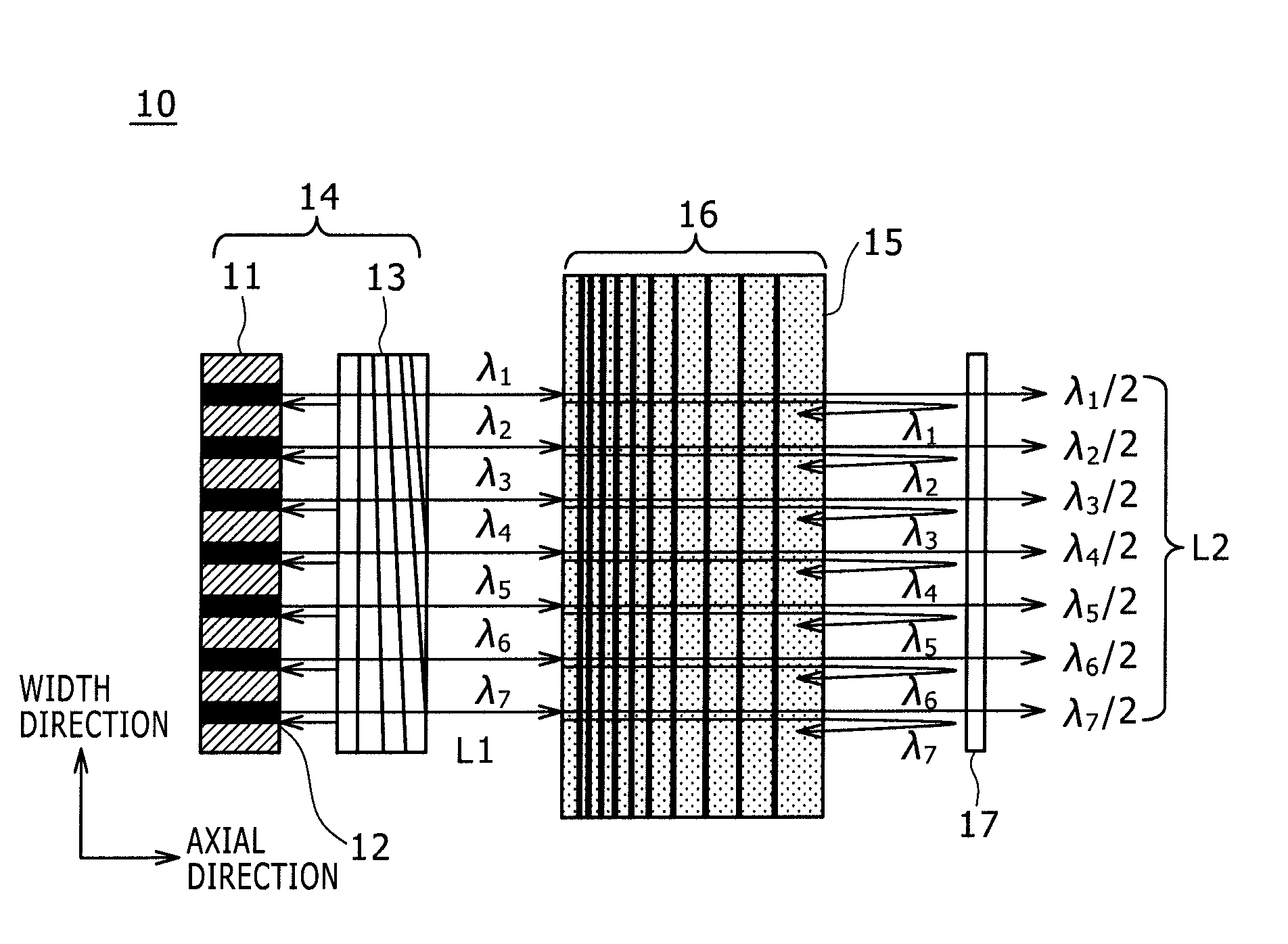
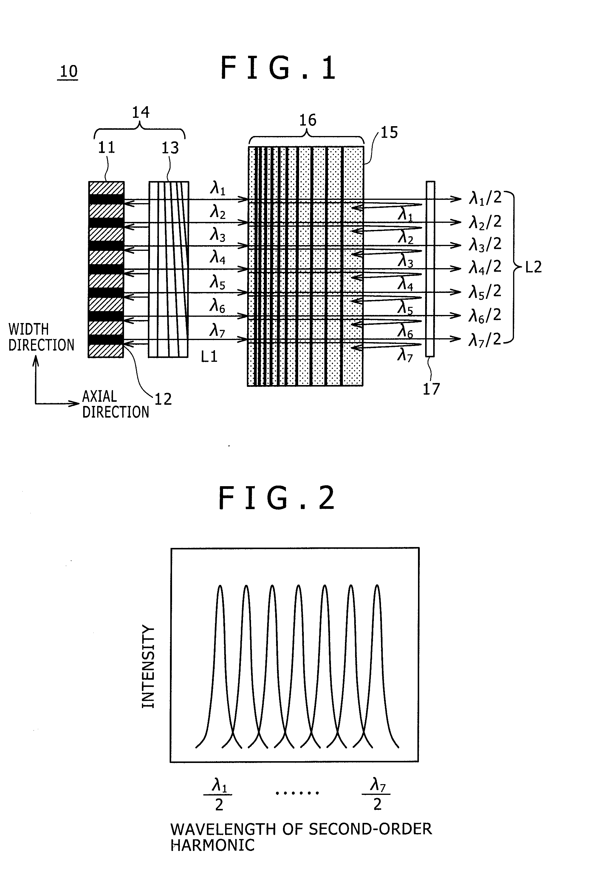
[0058]FIG. 1 is a schematic view showing a structure of a laser device according to a first embodiment of the present invention. As shown in FIG. 1, the laser device 10 includes a fundamental wave generating portion 14 composed of a semiconductor laser 11 composed of a laser array having a plurality of luminous points 12, and a Bragg reflection structure 13. The fundamental wave generating portion 14 is structured in such a way that a plurality of fundamental waves having respective wavelengths which are different from each other in at least one set thereof are generated. In addition, a nonlinear optical element 15 is disposed in a direction along which a plurality of fundamental waves L1 are emitted from the fundamental wave generating portion 14. A poling structure 16 adapted to pseudophase matching for the wavelengths of the fundamental waves L1 is formed along re...

second embodiment

2. Second Embodiment

The Second Case where the Poling Period and the Poling Duty Ratio Change in the Propagating Direction

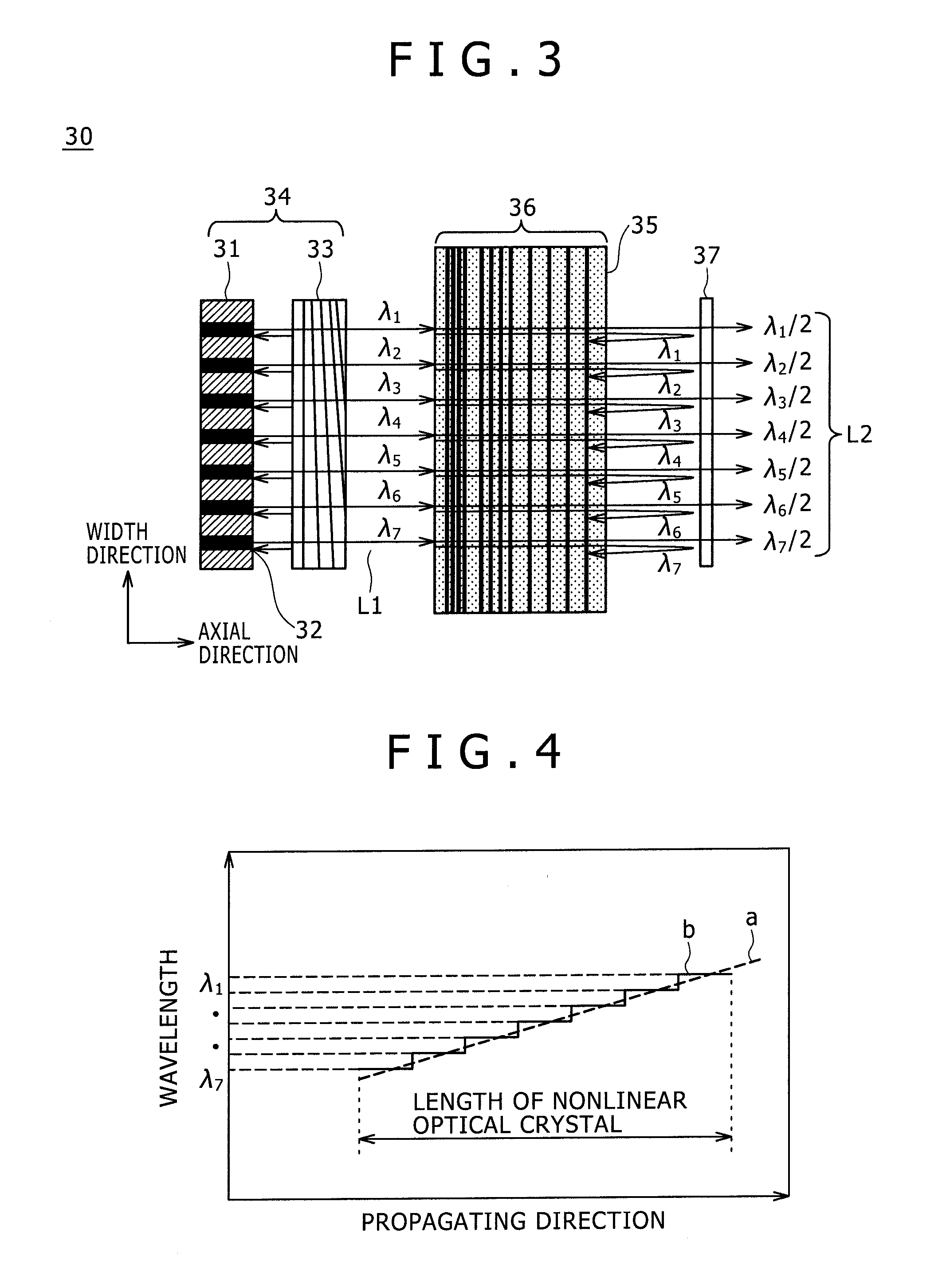
[0080]FIG. 3 is a schematic view showing a structure of a laser light source device 30 according to a second embodiment of the present invention.

[0081]In the laser device 30, a fundamental wave generating portion 34 is composed of a semiconductor laser 31 composed of a semiconductor laser array or the like and having a plurality of luminous points 32, and a Bragg reflection structure 33. Also, the fundamental wave generating portion 34 generates a plurality of fundamental waves L1 having respective wavelengths λ1, λ2, . . . λ7 which are different from each other in at least one set thereof. In addition, a nonlinear optical element 35 having a poling structure 36, and a filter 37 for transmitting the harmonics and reflecting the fundamental waves are disposed in a traveling direction of the fundamental waves L1 generated.

[0082]The nonlinear optical element 35 in th...

third embodiment

3. Third Embodiment

The Case where the Poling Period Changes in the Propagating Direction and in the Laser Array Arrangement Direction

[0093]FIG. 7 is a schematic view showing a structure of a laser device 40 according to a third embodiment of the present invention.

[0094]The laser device 40 includes a fundamental wave generating portion 44 composed of a semiconductor laser array 41 and a Bragg reflection structure 43. In this case, the semiconductor laser array 41 has a plurality of luminous points 42. Also, the Bragg reflection structure 43 stabilizes the laser beams emitted from the semiconductor laser array 41 into a plurality of fundamental waves L1 having respective wavelengths λ1, λ2, . . . , λ7 which are different from each other in at least one set thereof. In addition, the laser device 40 includes a nonlinear optical element 45 and a filter 47. In this case, the nonlinear optical element 45 has a poling structure 46 meeting the pseudophase matching condition for a plurality o...


PUM


Abstract

A laser device, includes: a fundamental wave generating portion configured to generate a plurality of fundamental waves having wavelengths which are different from each other in at least one set thereof, the fundamental wave generating portion having a semiconductor laser having a plurality of luminous points, and a Bragg reflection structure; and a nonlinear optical element in which a poling structure adapted to pseudophase matching for the wavelengths of the plurality of fundamental waves emitted from the fundamental wave generating portion, respectively, is formed variatively along a propagating direction of the plurality of fundamental waves.

Description

[0001]The present application claims priority to Japanese Patent Application JP 2009-047028 filed in the Japan Patent Office on Feb. 27, 2009, the entire content of which is hereby incorporated by reference.BACKGROUND OF THE INVENTION[0002]1. Field of the Invention[0003]The present invention relates to a laser device which wavelength-converts laser beams emitted from either a semiconductor laser having a plurality of luminous points, or a semiconductor having a longitudinal multimode, a laser display apparatus, a laser radiating apparatus, and a nonlinear optical element.[0004]2. Description of the Related Art[0005]A laser light source is useful as a light source for a projection display which has a wide color gamut, high color purity and a high efficiency. Thus, the laser light source can provide an image which is of high quality in terms of a color reproducibility, minute expression, a local luminance and the like. However, since a laser beam emitted from the laser light source is...

Claims


Application Information

Patent Timeline
IPC IPC(8): G02F1/37H01S3/10H01S3/08G02F1/35G02B27/48G02F1/29
CPCG02B26/123G02B27/0031G02B27/1006G02B27/104G02B27/145G02B27/48G02F2203/58G02F1/37G02F2001/3548H01S5/0092H01S5/141H01S5/4087G02F1/3544G02F1/3548
Inventor KIMURA, KAORUFURUKAWA, AKIOOKA, MICHIO
Owner SONY CORP
Why Eureka
Try Eureka