Nitride Semiconductor Light Emitting Element

a light-emitting element and nitride technology, applied in the direction of basic electric elements, semiconductor devices, electrical equipment, etc., can solve the problems of difficult manufacturing of nitride semiconductor bulk single crystals, difficult forming of two electrodes to sandwich a sapphire substrate, and difficulty in uniform current injection into the active layer, etc., to achieve wider irradiation angle and high light extraction efficiency

Active Publication Date: 2010-09-09
ROHM CO LTD
View PDF4 Cites 16 Cited by
  • Summary
  • Abstract
  • Description
  • Claims
  • Application Information

AI Technical Summary

Benefits of technology

[0017]In the present invention, the use of n type nitride semiconductor layer as the anti-reflection layer is made to be accompanied by the use of p type nitride semiconductor layer as the Bragg reflection layer, or the use of n type nitride semiconductor layer as the Bragg reflection layer is made to be accompanied by th

Problems solved by technology

Bulk single crystals for the nitride semiconductors, however, are difficult to be manufactured.
The sapphire substrates, however, are insulating substrates, and are not electrically conductive.
Accordingly, forming two electrod

Method used


Image

  • Nitride Semiconductor Light Emitting Element
  • Nitride Semiconductor Light Emitting Element
  • Nitride Semiconductor Light Emitting Element

Examples


Embodiment Construction

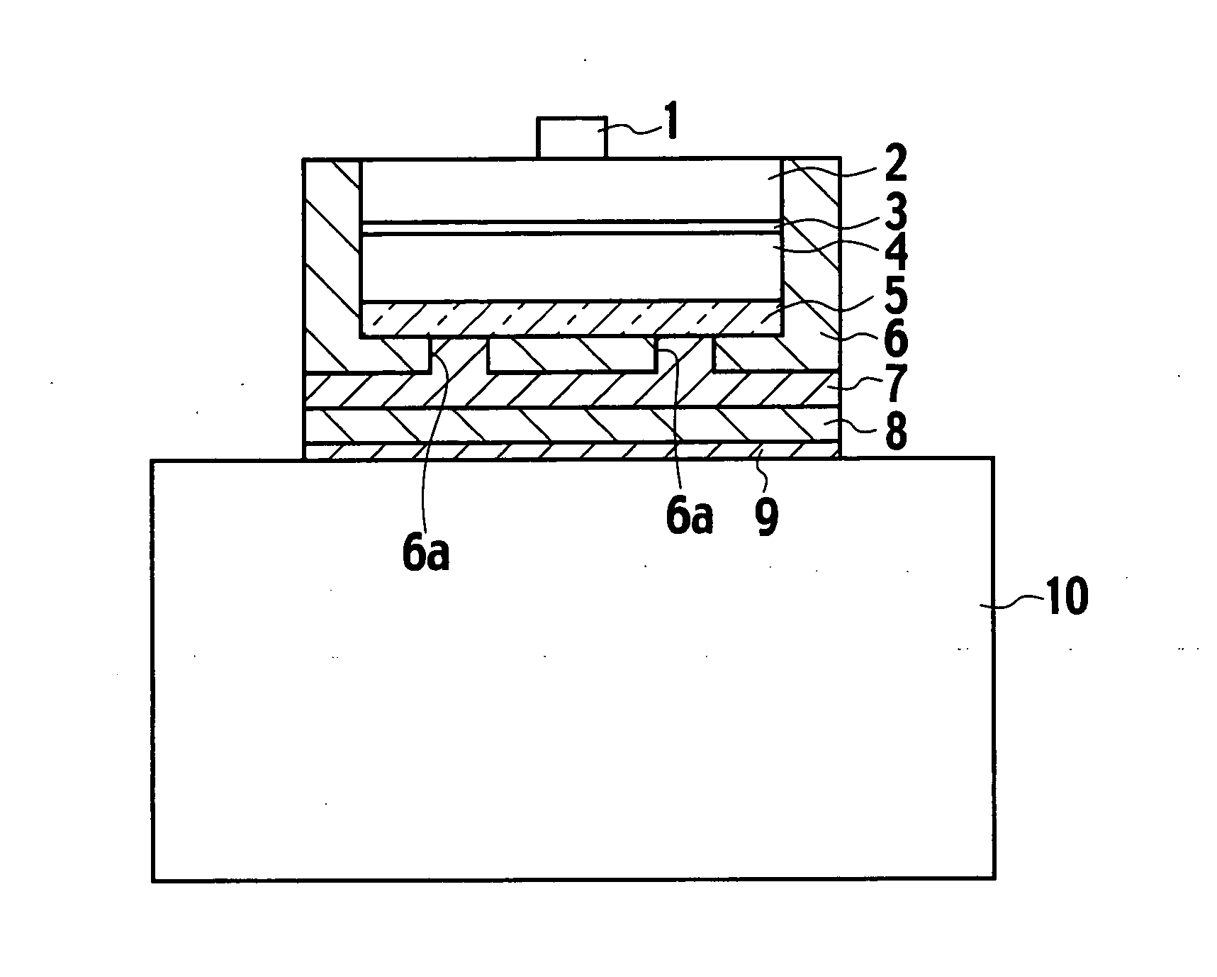
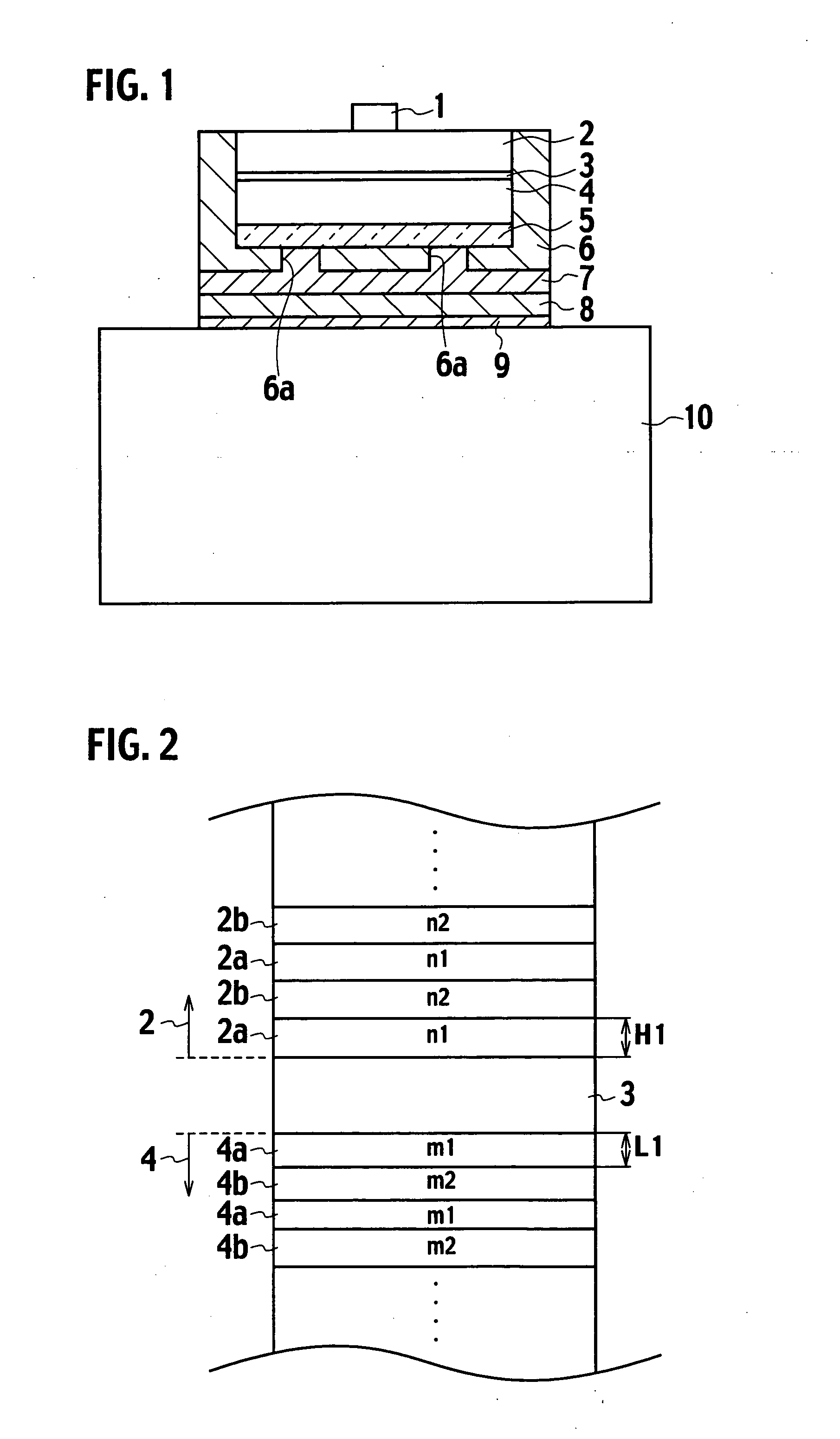
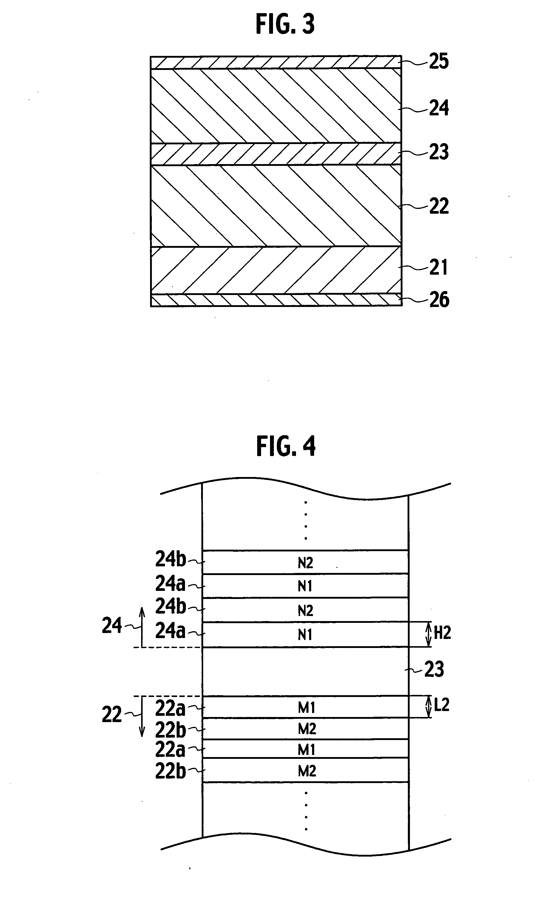
[0040]An embodiment of the present invention will be described below with reference to the drawings. FIG. 1 illustrates a structure of a nitride semiconductor light emitting element according to the present invention.

[0041]The nitride semiconductor light emitting element has a double hetero structure in which an n side anti-reflection layer 2 and p side Bragg reflection layer 4 are formed so as to sandwich an MQW active layer 3 that serves as a light-emitting region. The MQW active layer 3 has a multiple quantum well structure formed with InGaN / GaN and the like. For example, a layered structure is formed with layers of In0.17GaN of a 30-Å thickness as the well layers and layers of undoped GaN of 100-Å thickness as barrier layers (blocking layers) that are alternated by eight cycles. Note that layers of InGaN with an In composition of a range from 0.5% to 2% may be used as the barrier layers.

[0042]An n type nitride contact layer is usually formed on an n type nitride semiconductor la...


PUM


Abstract

Provided is a nitride semiconductor light emitting element that has improved light extraction efficiency and a wide irradiation angle of outgoing light irrespective of the reflectance of a metal used for an electrode. An n side anti-reflection layer 2 and a p side Bragg reflection layer 4 are formed so as to sandwich an MQW active layer 3 that serves as a light emitting region, and the nitride semiconductor light emitting element has a double hetero structure. On top of the n side anti-reflection layer 2, an n electrode 1 is formed. Meanwhile, at the lower side of the p side Bragg reflection layer 4, a p electrode 5, a reflection film 7, and a pad electrode 8 are formed, and the pad electrode is bonded to a support substrate 10 with a conductive bonding layer 9 interposed in between. Both the n side anti-reflection layer 2 and the p side Bragg reflection layer 4 also serve as contact layers. The n side anti-reflection layer 2 is disposed on the light-extracting-direction side while the p side Bragg reflection layer 4 is disposed on the opposite side to the light-extracting-direction side. Consequently, the light extraction efficiency is improved.

Description

TECHNICAL FIELD[0001]The present invention relates to a nitride semiconductor light emitting element that has improved light extraction efficiency.BACKGROUND ART[0002]Nitride semiconductors are used for: for example, blue LEDs, which are used as light sources of illumination, backlights, or the like; multi-color LEDs; LDs; and the like. Bulk single crystals for the nitride semiconductors, however, are difficult to be manufactured. Instead, GaN is grown on a substrate for growth, such as a sapphire substrate and a SiC substrate, by the MOCVD (metal organic chemical vapor deposition) method.[0003]Above all, sapphire substrates, which exhibit an excellent stability in the high-temperature ammonia atmosphere of the epitaxial growth process, are particularly used as substrates for growth. The sapphire substrates, however, are insulating substrates, and are not electrically conductive. Accordingly, forming two electrodes to sandwich a sapphire substrate is impossible. For this reason, to ...

Claims


Application Information

Patent Timeline
IPC IPC(8): H01L33/46H01L33/06H01L33/10H01L33/32
CPCH01L33/10H01L33/44H01L33/405H01L33/32
Inventor NAKAHARA, KEN
Owner ROHM CO LTD
Why Eureka
Try Eureka