Stacked device assembly with integrated coil and method of forming same

a technology of integrated coils and stacked devices, applied in the direction of magnetic bodies, magnetic device details, magneticonductors/solid-state devices, etc., can solve the problems of limiting the inductance of manufacturers, affecting the performance of manufacturers, and having undesirable characteristics

Inactive Publication Date: 2010-09-09
TAIWAN SEMICON MFG CO LTD
View PDF15 Cites 24 Cited by
  • Summary
  • Abstract
  • Description
  • Claims
  • Application Information

AI Technical Summary

Problems solved by technology

Unfortunately, however, the small dimensions of such planar inductors limit their inductance.
In addition, they can possess characteristics that are undesirable.
This electromagnetic flux can cause adverse affects.
However, the inductance value of the non-...

Method used


Image

  • Stacked device assembly with integrated coil and method of forming same
  • Stacked device assembly with integrated coil and method of forming same
  • Stacked device assembly with integrated coil and method of forming same

Examples


Embodiment Construction

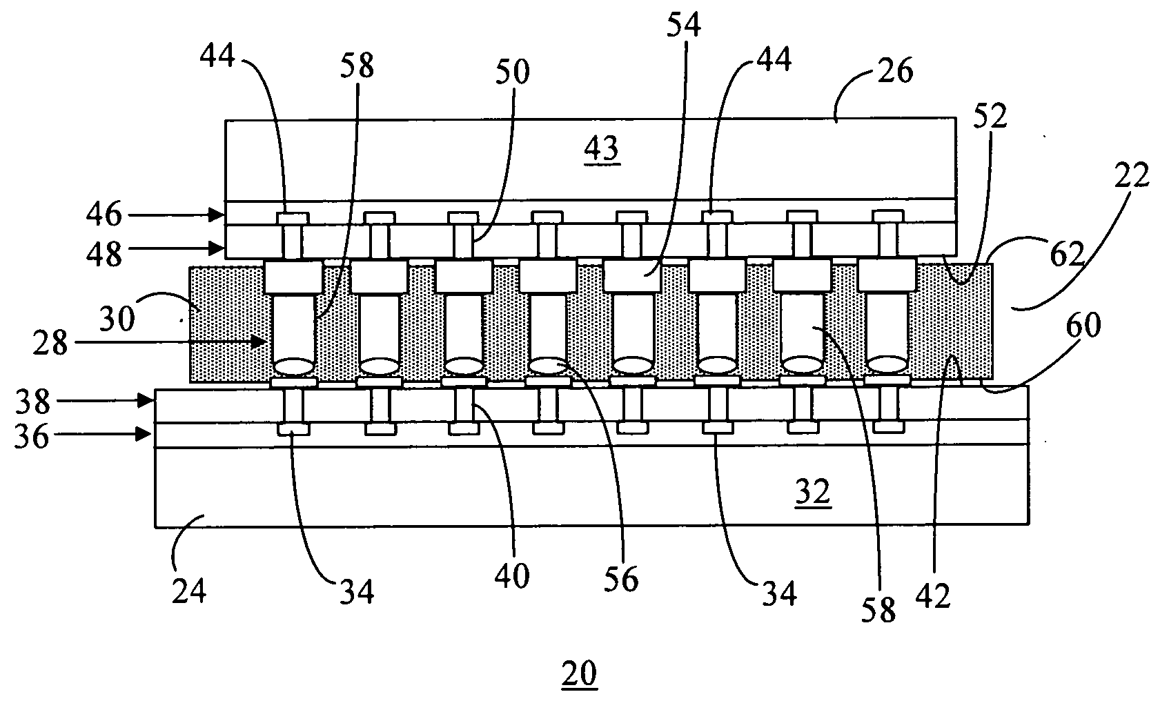
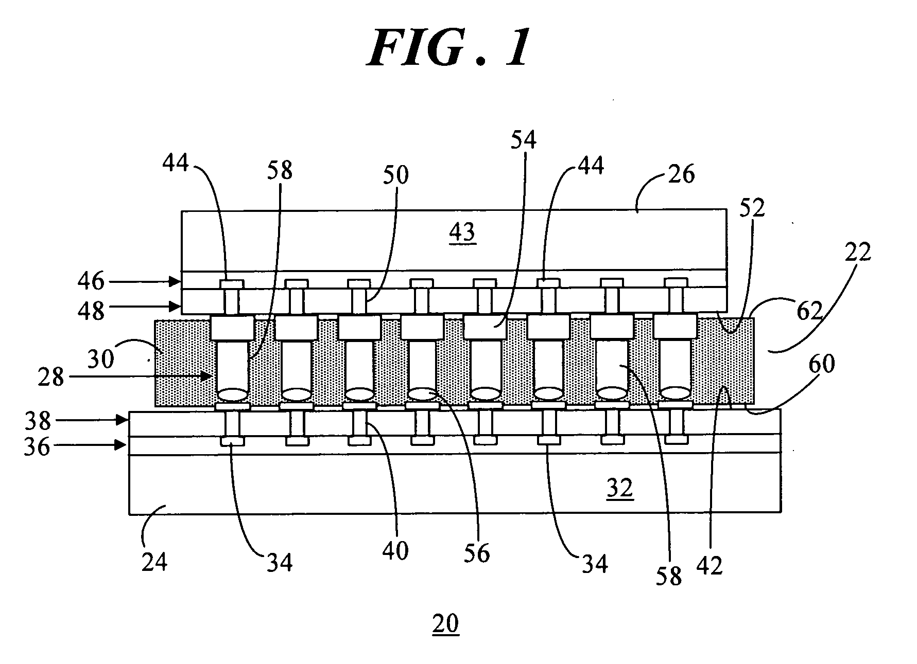
[0022]A stacked semiconductor device assembly can include a non-planar device coil that may be implemented to form a non-planar inductor. In an aspect, the stacked device assembly includes conductive traces formed in a first semiconductor device and conductive traces formed in a second semiconductor device. Conductive interconnects interconnect the conductive traces of the first semiconductor device with the conductive traces of the second semiconductor device to form a continuous device coil formed from alternating the electrical connection of the conductive traces of the first device with the conductive traces of the second device. In accordance with an embodiment, a large value non-planar inductor can be formed in a stacked semiconductor device assembly through the implementation of the two sets of conductive traces having a fine pitch combined with strategically oriented conductive interconnects having a larger pitch. Inductance values greater than 100 nanohenries, and more part...


PUM

PropertyMeasurementUnit
Electrical conductoraaaaaaaaaa
Magnetismaaaaaaaaaa

Abstract

A stacked semiconductor device assembly (20) includes a device (24) having conductive traces (34) formed therein, and conductive interconnects (28) electrically connected to the conductive traces (34). Another device (26) has conductive traces (44) formed therein and device pads (54) formed on an outer surface (52) of the device (26). A method (120) entails attaching (84) a magnetic core (30) to an outer surface (42) of the device (24) and forming (92) the conductive interconnects (28) on the outer surface (42) using a stud bumping technique such that the interconnects (28) surround the magnetic core (30). The conductive interconnects (28) are coupled (126) with the device pads (54) using thermocompression bonding to couple the device (26) with the device (24) to form a continuous device coil (22) wrapped around the magnetic core (30) from an alternating electrical connection of the traces (34), the conductive interconnects (28), and the traces (44).

Description

TECHNICAL FIELD OF THE INVENTION [0001]The present invention relates generally to electronic devices and processes. More specifically, the present invention relates to electronic devices that include device coils, such as inductors, transformers, and the like, and processes of forming the same.BACKGROUND OF THE INVENTION [0002]A “system-in-a-package” (SIP) or a “chip stack,” refers to a semiconductor device that incorporates multiple chips that make up a complete electronic system enclosed in a single package or module. In an SIP, dies containing integrated circuits may be stacked vertically. They are internally connected by fine wires that are bonded to the package. Alternatively, with a flip chip technology, solder bumps may be used to join stacked chips together.[0003]An exemplary SIP can contain several chips, such as a specialized processor, dynamic random access memory (DRAM), flash memory, and so forth, combined with passive components, such as resistors, capacitors, and the ...

Claims


Application Information

Patent Timeline
IPC IPC(8): H01F5/00H01R43/00
CPCH01F17/0013Y10T29/49117H01F27/2804H01F2017/002H01F2027/2814H01L23/645H01L24/11H01L24/13H01L24/17H01L24/81H01L24/94H01L24/97H01L25/0657H01L25/50H01L2224/32145H01L2224/81203H01L2224/81801H01L2224/97H01L2225/06527H01L2225/06586H01L2924/01013H01L2924/01029H01L2924/01032H01L2924/01046H01L2924/01077H01L2924/01078H01L2924/01079H01L2924/01082H01L2924/01327H01L2924/14H01L2924/19041H01L2924/19042H01L2924/19104H01F17/04Y10T29/4902H01L2924/1461H01L2924/07802H01L2224/73204H01L2224/81013H01L2924/01033H01L2924/01044H01L2924/01045H01L2924/01076H01L2224/81012H01L2224/81011H01L2224/81H01L2924/00H01L2924/12044H01L2224/1134H01L2224/13144H01L2224/05026H01L2224/0557H01L2224/05568H01L2224/05001H01L2224/05124H01L2224/05147H01L2224/05644H01L2224/05664H01L2224/05669H01L24/16H01L2224/0616H01L2924/00014
Inventor WANG, JAMES JEN-HOD'ACOSTA, CARL E.POARCH, JUSTIN E.
Owner TAIWAN SEMICON MFG CO LTD
Why Eureka
Try Eureka