

SRAM and testing method of SRAM
a testing method and memory cell technology, applied in the field of sram and a testing method of sram, can solve the problem that the abnormal state of memory cells cannot be detected, and achieve the effect of suppressing the increase in the circuit area of sram and improving the detection sensibility of abnormal memory cells
- Summary
- Abstract
- Description
- Claims
- Application Information
AI Technical Summary
Benefits of technology
Problems solved by technology
Method used
Image

Examples
first embodiment
[0042]The SRAM according to a first embodiment of the present invention and a read test method for the SRAM will be described below with reference to FIGS. 5 and 6.
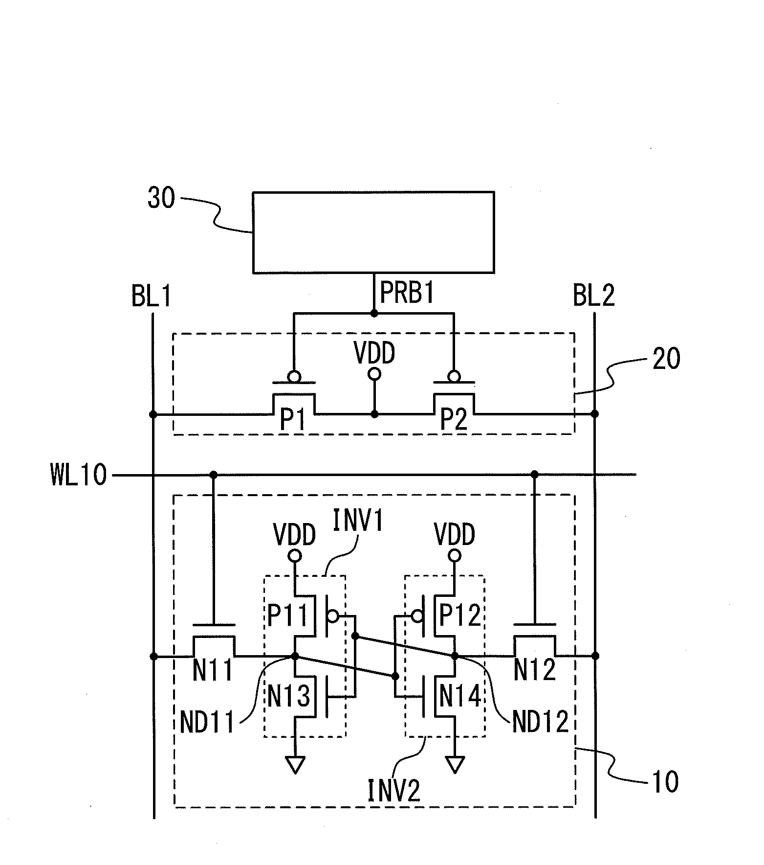
[0043]FIG. 5 is a circuit diagram showing a part of the configuration of the SRAM in the first embodiment. The SRAM in the first embodiment contains a memory cell 10, which is connected to bit lines BL1 and BL2 and a word line WL10, a pre-charging circuit 20 for pre-charging the bit lines BL1 and BL2; and a pre-charge control circuit 30 for controlling the pre-charging circuit 20. The pre-charge control circuit 30 also controls a pre-charging circuit connected to another bit line pair (not shown).
[0044]With reference to FIG. 5, the memory cell 10 contains a positive feedback loop (flip-flop) of two CMOS inverters INV1 and INV2; and two N-channel MOS transistors N11 and N12 (hereinafter, to be referred to as selection transistors N11 and N12) for controlling the connections between the bit lines BL1 and BV2 and the inverte...
second embodiment
[0071]The SRAM according to a second embodiment of the present invention and the read test method of the SRAM will be described below with reference to FIGS. 10 to 13A. FIG. 10 is a circuit diagram showing a part of the configuration of the SRAM in the second embodiment. In the SRAM in the first embodiment, in the test mode, the pre-charging circuit 20 is controlled by changing the signal level of a pre-charge control signal PB1 to any value (the voltage Vg). Accordingly, a predetermined voltage between the high level and the low level is biased to the bit lines BL1 and BL2, and the data of the memory cell whose SNM is small is forcedly inverted. Thus, it is made possible to detect the memory cell in the abnormal state that cannot be usually rejected. On the other hand, in the SRAM in the second embodiment, in the test mode, the signal level of the selection signal outputted to the word line is changed to any value to control the pull-up performance of the holding node in the memory...
third embodiment
[0099]The third embodiment of the SRAM according to the present invention and the read test method of the SRAM will be described below with reference to FIGS. 15 to 18.
[0100]FIG. 15 is a circuit diagram showing a part of the configuration of the SRAM in the third embodiment. In the SRAM in the third embodiment, the power supply voltage supplied to the memory cell is changed to any value in the test mode, to control the pull-up performance of the holding node in the memory cell. Consequently, the data of the memory cell whose SNM is small is forcedly inverted, which allows the detection of the memory cell in the abnormal state that cannot be usually rejected.
[0101]The configuration of the SRAM in the third embodiment will be described below with reference to FIG. 15. Here, the same symbols are assigned to the same components in the first embodiment, and their explanations are omitted. The SRAM in the third embodiment contains the memory cell 10, the pre-charging circuit 20 and a powe...
PUM
 Abstract
Description
Claims
Application Information