Vibration compensation in probe microscopy

a probe microscopy and vibration compensation technology, applied in the field of vibration compensation in the probe microscopy, can solve the problems of inability to produce absolute deflection measurements of the measurement probe, limited resolution, and limited afm, and achieve the effect of constant deflection of the scanning probe and constant interaction

Active Publication Date: 2010-09-16
INFINITESIMA
View PDF3 Cites 16 Cited by
  • Summary
  • Abstract
  • Description
  • Claims
  • Application Information

AI Technical Summary

Problems solved by technology

Inevitably this spatial relationship is affected, and thus the resolution is limited, by amongst other things the operating environment and in particular mechanical and acoustic noise which generate an uncertainty in the position of the probe relative to the specimen.
However, the AFM is restricted to differential deflection data; no absolute deflection measurements of the measurement probe can be produced using this microscope.
However, as a result of the common position control, the height reference measurement of the distance sensor is not independent of the scanning measurements.
Semiconductor device fabrication involves highly complex techniques for constructing integrated circuits using semiconductor materials.
Due to the large scale of circuit integration and the decreasing size of semiconductor devices, the semiconductor fabrication process is prone to processing defects.
However, such optical devices are limited in their ability to analyze and accurately identify defect types on a semiconductor wafer.
However, scanning electron microscopy has the disadvantage that not only must the wafers be removed from the production line; they have to be transferred to an evacuated enclosure for the purposes of electron microscopy.
This can add considerable time to the inspection and review procedure, which increased time is undesirable.
Moreover, scanning electron microscopy can result in damage to the wafer surface via beam damage and / or contamination.
However, due to the length of time required to produce a surface scan using conventional scanning probe microscopy apparatus, the application of such microscopy techniques is limited in large-scale wafer fabrication.
Moreover, as with all local probe techniques, the resolution and capabilities of such local probe microscopy apparatus are directly affected by environmental mechanical vibrations, especially where a local probe is mounted in a conventional inspection / review tool.
Additionally, the need to move and reposition the sample, e.g. a wafer, introduces mechanical vibrations which must settle before a measurement can be collected and this reduces throughput.
However, microscopes employing these noise compensation techniques require two separate measurement systems and are thus costly.
More importantly the interferometers are only capable of measuring displacements, representative of noise amplitudes, of less than half a wavelength.

Method used


Image

  • Vibration compensation in probe microscopy
  • Vibration compensation in probe microscopy
  • Vibration compensation in probe microscopy

Examples


Embodiment Construction

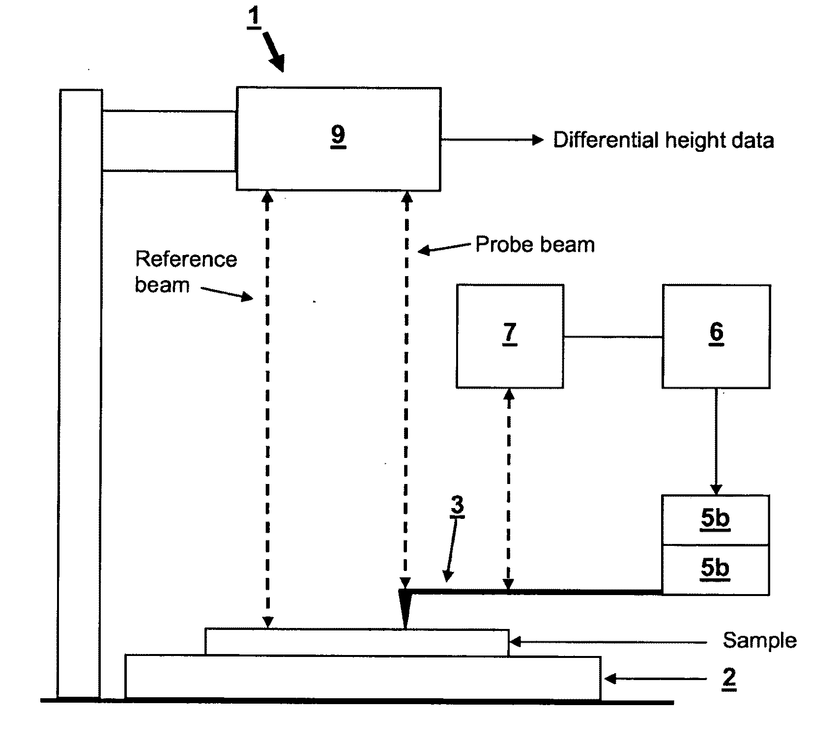
[0039]FIG. 1 illustrates scanning probe microscopy (SPM) apparatus 1 including noise compensation apparatus. The apparatus 1 shown in FIG. 1 includes a sample stage 2, adapted to receive a sample. A probe 3 is mechanically connected to x, y, and z translation stages 5a for controlling fine movement of the probe 3 in all three orthogonal directions. The translation stages preferably comprise a set of piezoelectric transducers arranged to effect independent movement of the probe in the three orthogonal directions. One or more separate coarse positioning drives 5b are also provided for driving the initial approach of the probe 3 to the sample on the sample stage 2. The coarse positioning drives 5b optionally consist of orthogonally arranged actuators. The coarse positioning drives 5b and the translation stages 5a are, in turn, in communication with and controlled by a controller 6. The translation stages 5a and positioning drives 5b provide fine and coarse positioning of the probe 3 re...


PUM


Abstract

A The local probe microscopy apparatus (1) comprises a probe (3) with translation stages (5a, 5b) for controlling the position of the probe (3) relative to a sample surface. The probe (3) has a feedback mechanism (6, 5 7) for maintaining the deflection of the probe and a height measuring system (9) which includes means for compensating for environmental noise. The local probe microscopy apparatus is particularly suitable for use as a wafer inspection tool in a wafer fabrication plant where the inspection tool is liable to be exposed to significant mechanical vibration.

Description

FIELD OF THE INVENTION[0001]The present invention generally relates to vibration compensation in probe microscopy and to a method of and apparatus for vibration compensation. The present invention is particularly, but not exclusively, suited for use in the inspection and / or review of semiconductor wafers and to a surface review tool for use in surveying and / or imaging specimen surfaces using a local probe. A particular type of local probe microscope and a field of application for which the invention is suitable is scanning force microscopy (SFM), also know as atomic force microscopy (AFM). However, it is to be understood that the invention is not restricted to such a field.BACKGROUND AND RELATED ART[0002]Local probe microscopy is capable of high-resolution non-destructive measurement of one or more characteristics of a specimen's surface. A typical AFM operated in contact mode includes a probe comprising a cantilever with a probe tip mounted near the free end of the cantilever. The ...

Claims


Application Information

Patent Timeline
Patent Type & Authority Applications(United States)
IPC IPC(8): G01Q20/02G01Q40/00G01Q70/04
CPCB82Y35/00G01Q70/04G01Q20/02
Inventor HUMPHRIS, ANDREW
Owner INFINITESIMA
Why Eureka
Try Eureka