Lighting Device

a technology of light-emitting elements and light-emitting tubes, which is applied in the direction of light-emitting support devices, discharge tubes luminescnet screens, lighting and heating apparatus, etc., can solve the problem that the light-emitting element is not easily deteriorated, and achieves the effect of not easily deteriorating the element, simple manufacturing process, and mass production

Inactive Publication Date: 2010-09-23
SEMICON ENERGY LAB CO LTD
View PDF16 Cites 23 Cited by
  • Summary
  • Abstract
  • Description
  • Claims
  • Application Information

AI Technical Summary

Benefits of technology

[0008]According to one embodiment of the present invention, an object is to reduce the thickness of a lighting device which uses an electroluminescent material. Alternatively, according to one embodiment of the present invention, an object is to simplify the structure of a lighting device which uses an electroluminescent material.
[0009]One embodiment of the present invention is a lighting device in which: a terminal electrically connecting a light-emitting element included in the lighting device to the outside is formed over the same surface of a substrate as the light-emitting element; and the terminal is formed at the center of the substrate while the light-emitting element is stacked. In addition, the lighting device has a structure in which the light-emitting element is not easily deteriorated.
[0017]The lighting device according to one embodiment of the present invention can be manufactured by a simple manufacturing process and therefore can be mass-produced. Further, since the lighting device according to one embodiment of the present invention has a structure in which element deterioration is not easily caused, a lighting device having long lifetime can be provided. In addition, in the lighting device according to one embodiment of the present invention, reduction in weight and film thickness is realized and electrical connection to an external power supply can be easily made; therefore, the lighting device can be used for various applications.

Problems solved by technology

In addition, the lighting device has a structure in which the light-emitting element is not easily deteriorated.

Method used


Image

  • Lighting Device
  • Lighting Device
  • Lighting Device

Examples


embodiment 1

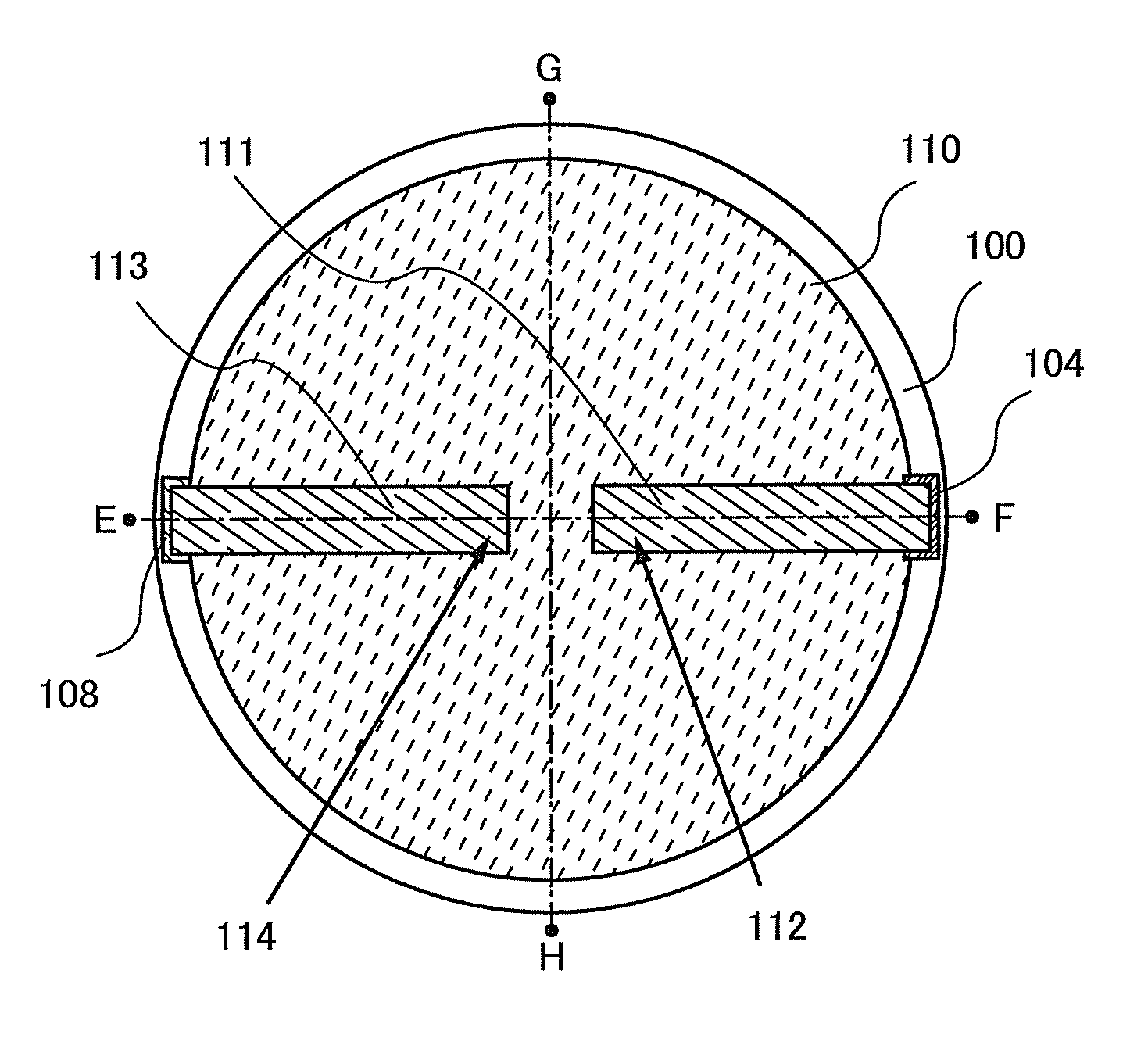
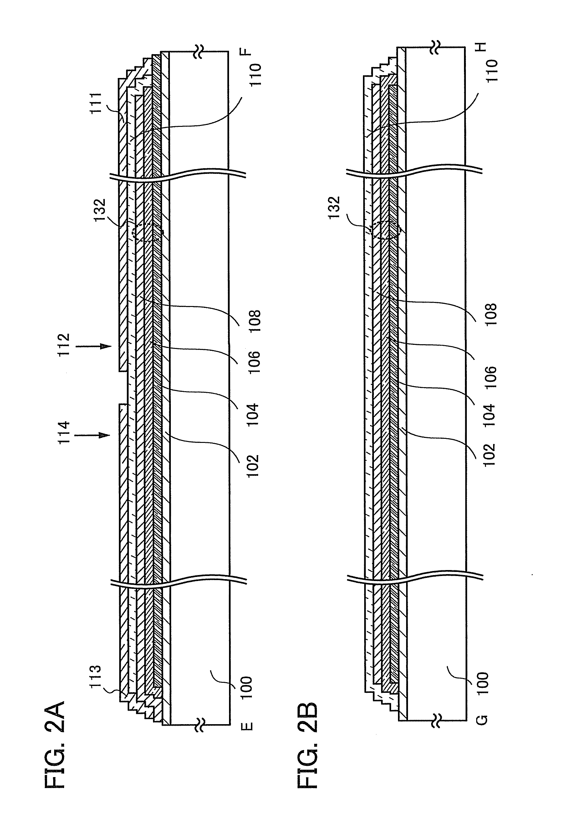
[0034]In Embodiment 1, one embodiment of a lighting device of the present invention will be described with reference to FIG. 1 and FIGS. 2A and 2B.

[0035]FIG. 1 is a plan view of a lighting device. FIG. 2A is a cross-sectional view taken along line E-F of FIG. 1 and FIG. 2B is a cross-sectional view taken along line G-H of FIG. 1.

[0036]A light-emitting element 132 including a first electrode layer 104, an EL layer 106, and a second electrode layer 108 is formed over a substrate 100 which is provided with an insulating film 102 as a base protective film (a barrier layer). An insulating film 110 covers the light-emitting element 132 except for part of the first electrode layer 104 and part of the second electrode layer 108. The insulating film 110 functions as a sealing film or a protective film which protects the EL layer 106 of the light-emitting element from external contaminants such as water. Note that the substrate 100 has a round shape (a disk shape, a discus shape, or a circula...

embodiment 2

[0056]In this embodiment, an example of a lighting device having a structure of an auxiliary wiring which is different from that of Embodiment 1 is described with reference to FIG. 3 and FIGS. 4A and 4B. That is, except the structure of the auxiliary wiring, the lighting device can be manufactured in a manner similar to Embodiment 1; thus, repetitive description of the same components as or components having functions similar to those in Embodiment 1 and manufacturing steps is omitted.

[0057]FIG. 3 is a plan view of the lighting device. FIG. 4A illustrates a cross-sectional view taken along line E-F of FIG. 3 and FIG. 4B illustrates a cross-sectional view taken along line G-H of FIG. 3.

[0058]A light-emitting element 132 including the first electrode layer 104, the EL layer 106, and the second electrode layer 108 is formed over the substrate 100 which is provided with the insulating film 102 as a base protective film. The insulating film 110 covers the light-emitting element 132 excep...

embodiment 3

[0069]In this embodiment, an example of a lighting device in which no auxiliary wiring is used is described with reference to FIG. 5 and FIGS. 6A and 6B. That is, except the absence of auxiliary wirings, the thin film transistor can be formed in a manner similar to Embodiment 1; thus, repetitive description of the same components as or components having functions similar to those in Embodiments 1 and 2 and manufacturing steps is omitted.

[0070]FIG. 5 is a plan view of the lighting device. FIG. 6A is a cross-sectional view taken along line X1-X2 of FIG. 5 and FIG. 6B is a cross-sectional view taken along line Y1-Y2 of FIG. 5.

[0071]The lighting device illustrated in FIG. 5 and FIGS. 6A and 6B is provided with a plurality of light-emitting elements: a light-emitting element 132a and a light-emitting element 132b, each of which has a semicircular shape. At the center of the substrate 100, the light-emitting element 132a has a first connecting portion 112a and a second connecting portion ...


PUM


Abstract

To reduce the thickness of a lighting device which uses an electroluminescent material and to simplify the structure of a lighting device which uses an electroluminescent material, in the lighting device of the present invention: a terminal electrically connecting a light-emitting element included in the lighting device to the outside is formed over the same surface of a substrate as the light-emitting element; and the terminal is formed at the center of the substrate while the light-emitting element is stacked. In addition, the lighting device has a structure in which the light-emitting element is not easily deteriorated.

Description

BACKGROUND OF THE INVENTION[0001]1. Field of the Invention[0002]One embodiment of the present invention relates to a lighting device including a light-emitting member which exhibits electroluminescence.[0003]2. Description of the Related Art[0004]As a next-generation lighting device, a lighting device using an electroluminescent material has attracted attention because it is estimated to have higher emission efficiency than filament bulbs or fluorescent bulbs. A thin film of an electroluminescent material can be formed to a thickness of 1 μm or less by evaporation or coating. Further, the structure of such a lighting device has been devised; for example, some inventions disclose a lighting device using an electroluminescent material in which the luminance is kept constant even when the area of the lighting device is increased (for example, see Patent Document 1).[0005]Further, in order to reduce the load on an electroluminescent panel, a lighting device is disclosed in which an elec...

Claims


Application Information

Patent Timeline
Patent Type & Authority Applications(United States)
IPC IPC(8): H05B33/06
CPCH05B33/22H05B33/28F21S8/03F21S8/04F21V21/002F21Y2105/00F21K9/20F21K9/23F21Y2115/20F21S41/155H10K50/11H10K50/156H01L33/02H01L33/62
Inventor YAMAZAKI, SHUNPEIARAI, YASUYUKISHIBATA, NORIKOSUZUKI, YUKIENAKAMURA, YASUOKAWAMATA, IKUKOMORIYA, YOSHITAKA
Owner SEMICON ENERGY LAB CO LTD
Why Eureka
Try Eureka