Semiconductor non-volatile memory, charge accumulating method for semiconductor non-volatile memory, charge accumulating program storage medium
- Summary
- Abstract
- Description
- Claims
- Application Information
AI Technical Summary
Benefits of technology
Problems solved by technology
Method used
Image

Examples
first exemplary embodiment
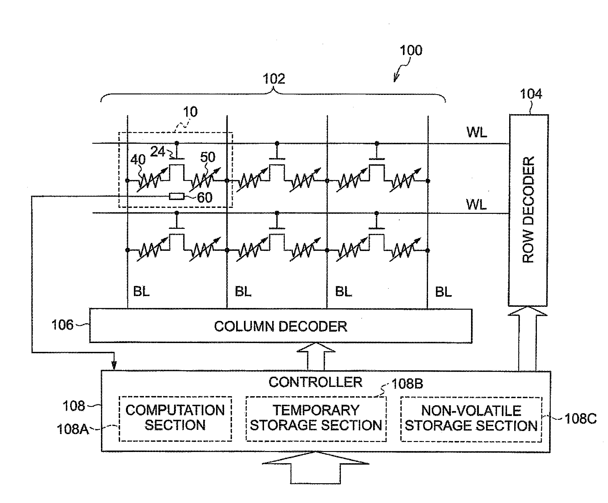
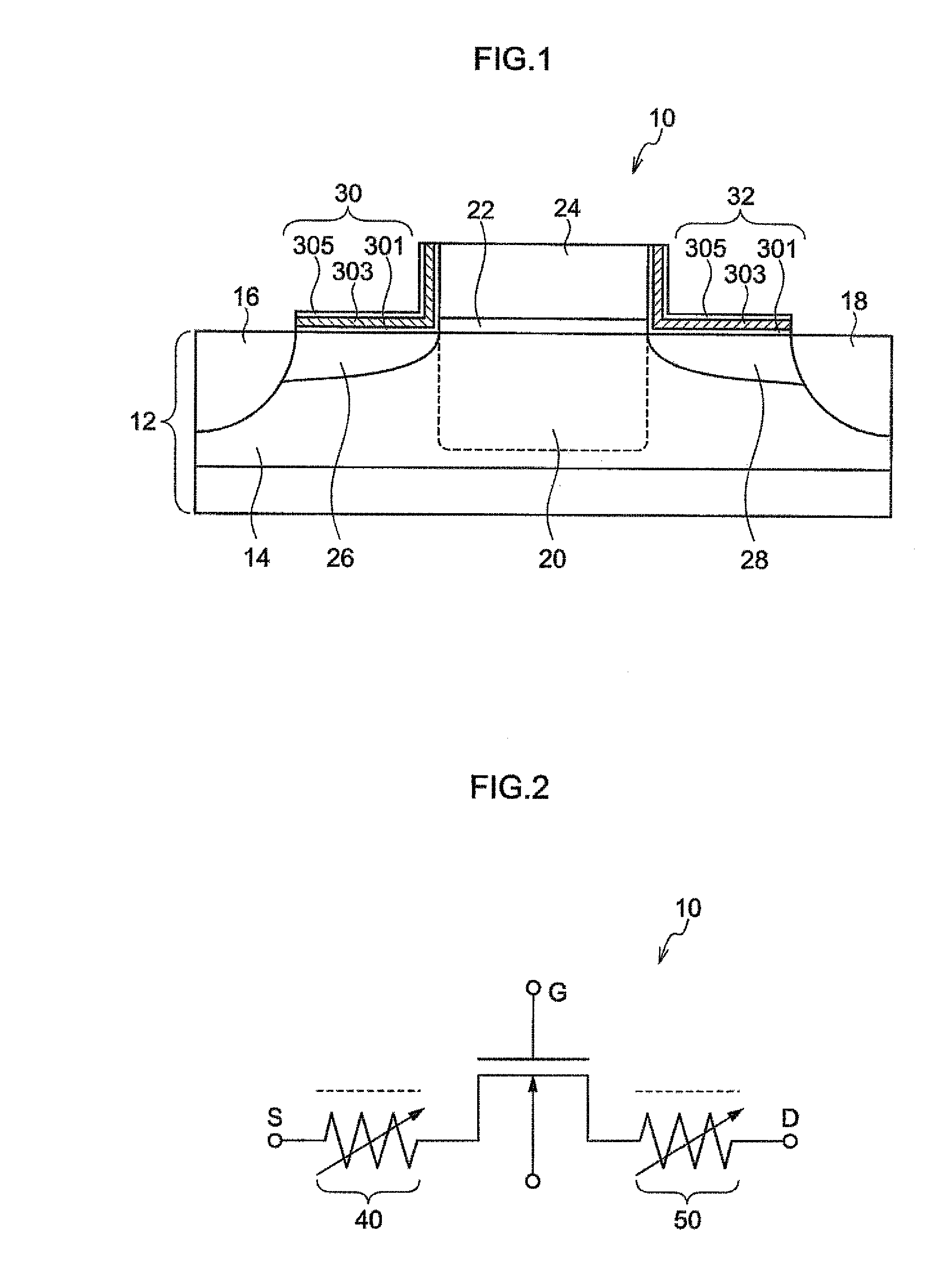
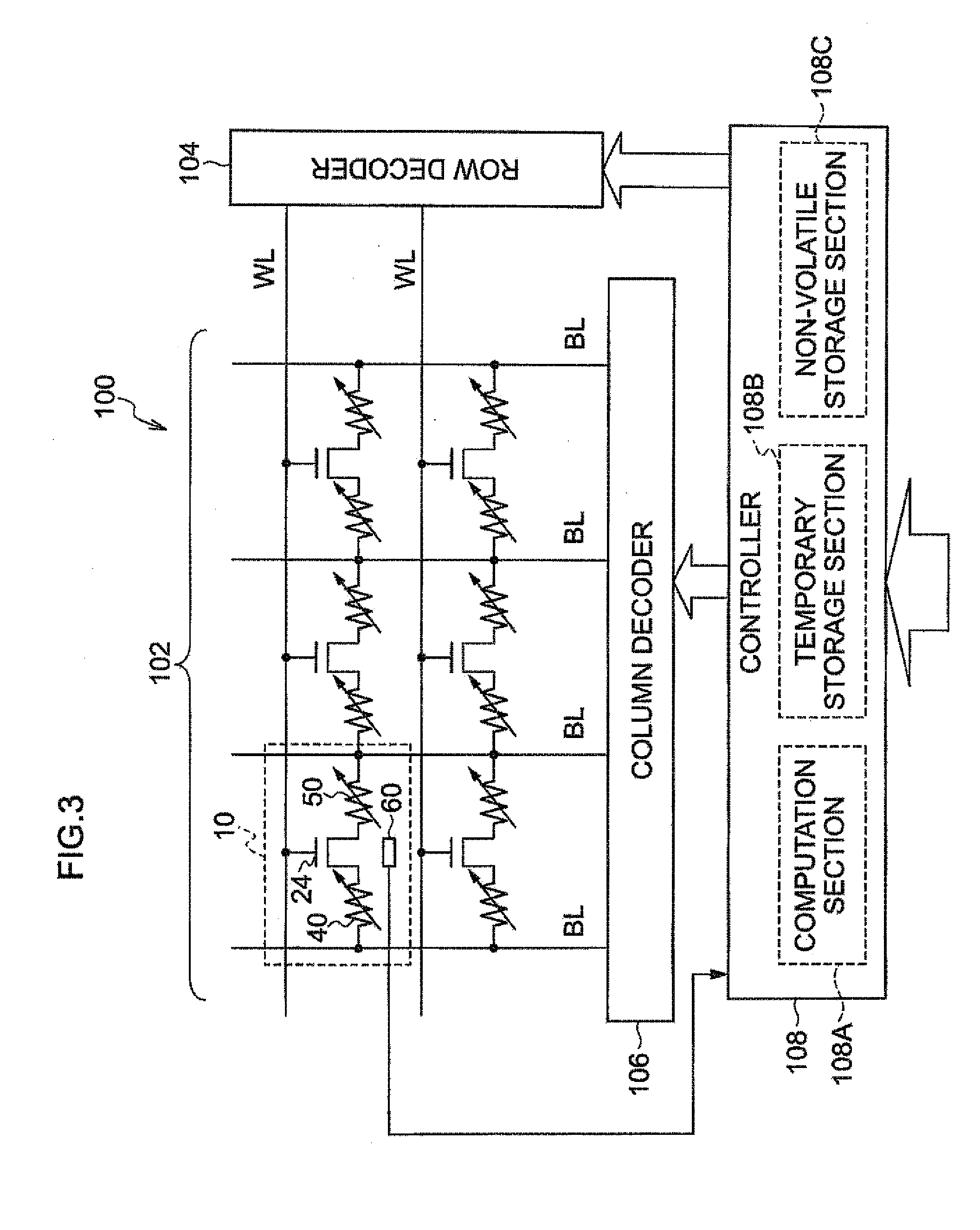
Structure of Memory Cell
[0116]FIG. 1 is a schematic cross-section diagram showing relevant parts of a memory cell 10 (memory section) configuring a semiconductor non-volatile memory of the present exemplary embodiment. Explanation follows in the present exemplary embodiment of an example of a case where the memory cell 10 is an n-type Metal Oxide Semiconductor Field Effect Transistor (n-MOSFET).
[0117]As shown in FIG. 1, the memory cell 10 is configured with a p-well region 14 formed on front face region side of a silicon substrate 12 (substrate), serving as a p-type semiconductor substrate. A source region 16 and a drain region 18, each including a high concentration of an n-type impurity (n+-type), are provided on surface regions of the p-well region 14, separated from each other by a specific separation distance. Note that the source region 16 and the drain region 18 are each provided with a metal electrode layer (not shown in the figures) with a contact layer (not shown in the fi...
second exemplary embodiment
[0231]Explanation follows of a second exemplary embodiment of the present invention. Since the configuration of the present exemplary embodiment is similar to the configuration of the above first exemplary embodiment, explanation thereof is omitted. Furthermore, there are also portions of the operation of the present exemplary embodiment that are similar to those of the first exemplary embodiment, so explanation is given below only of the differing portions thereof.
[0232]Namely, the steps 300M to 500M of FIG. 4 are executed similarly to in the above first exemplary embodiment. Namely, as shown in FIG. 20A, 00 data is written in sequence to each of plural memory cells, 01 data is written in sequence to each of plural memory cells, and 10 data is written in sequence to plural memory cells.
[0233]Furthermore, in the present exemplary embodiment too, processing is executed similar to the processing shown in FIG. 5 (FIG. 6, FIG. 7). Furthermore, in the present exemplary embodiment too, su...
PUM
 Abstract
Description
Claims
Application Information
 - R&D Engineer
- R&D Manager
- IP Professional
- Industry Leading Data Capabilities
- Powerful AI technology
- Patent DNA Extraction
Browse by: Latest US Patents, China's latest patents, Technical Efficacy Thesaurus, Application Domain, Technology Topic.
© 2024 PatSnap. All rights reserved.Legal|Privacy policy|Modern Slavery Act Transparency Statement|Sitemap