Applying Charge Pump To Realize Frequency Jitter For Switched Mode Power Controller

a power controller and charge pump technology, applied in the direction of pulse generator, pulse technique, electric pulse generator circuit, etc., can solve the problems of affecting the operation of other radio frequency operating equipment such as radio or television receivers, cumbersome analog emi filter approach, and large system area for mounting passive components, so as to reduce emi emission

Active Publication Date: 2010-09-30
BCD SHANGHAI MICRO ELECTRONICS CO LTD
View PDF2 Cites 20 Cited by
  • Summary
  • Abstract
  • Description
  • Claims
  • Application Information

AI Technical Summary

Benefits of technology

[0009]Embodiments of the present invention provide apparatus and method that use a charge pump circuit to generate a low frequency voltage having a triangular waveform. The low frequency voltage varies the frequency of a primary cloc

Problems solved by technology

However, the relative high switching frequency can be coupled back to the AC power line and interfere with the operation of other radio frequency operating equipment such as radio or television receivers.
The analog EMI filter approach not only is cumbersome because it requires numerous trials of different inductors and filters (i.e., on a trial-and-error basis), but also is expensive and requires large system area for mounting the passive components.
Furthermore, passive filters consumes additional

Method used


Image

  • Applying Charge Pump To Realize Frequency Jitter For Switched Mode Power Controller
  • Applying Charge Pump To Realize Frequency Jitter For Switched Mode Power Controller
  • Applying Charge Pump To Realize Frequency Jitter For Switched Mode Power Controller

Examples


Embodiment Construction

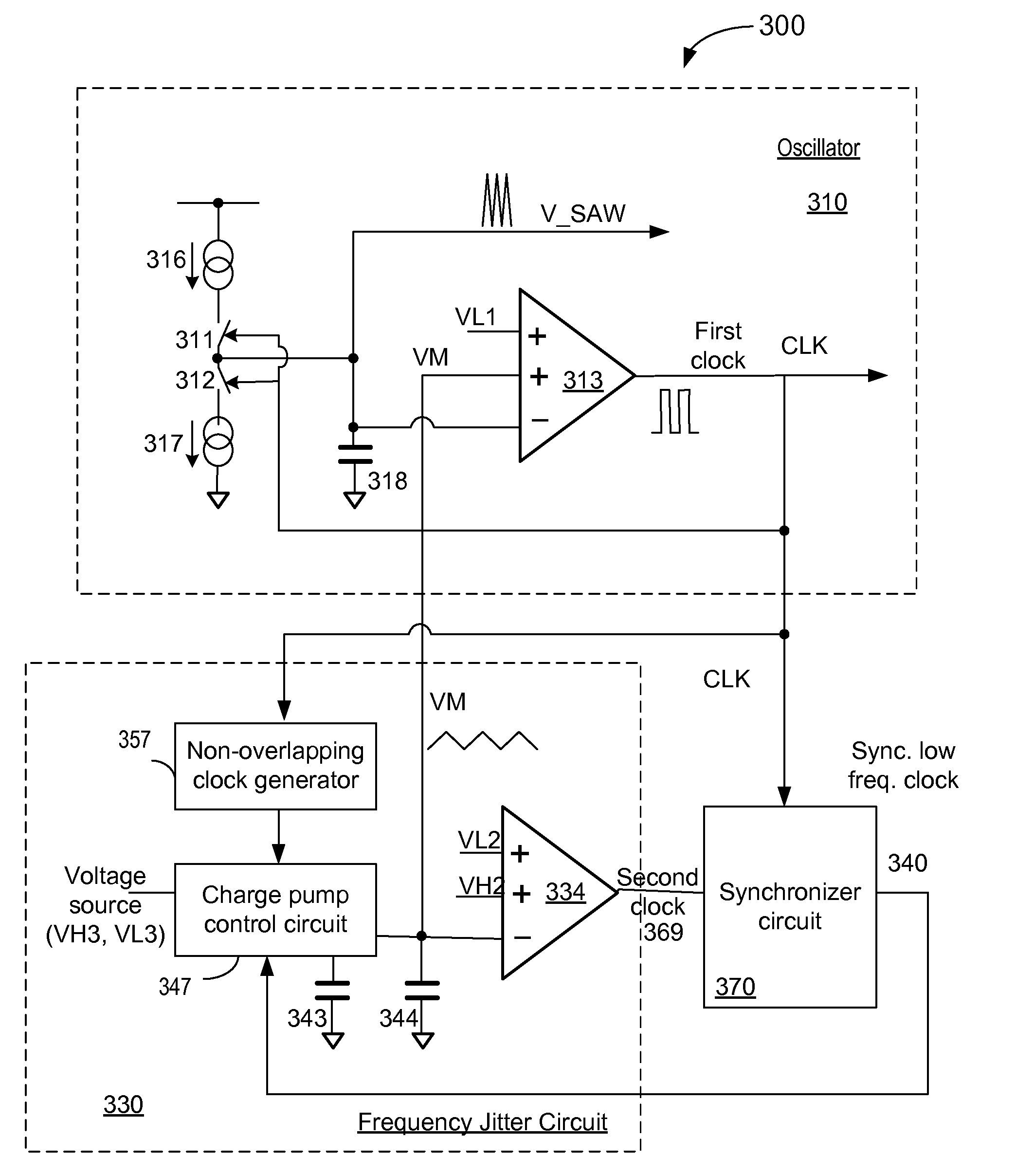
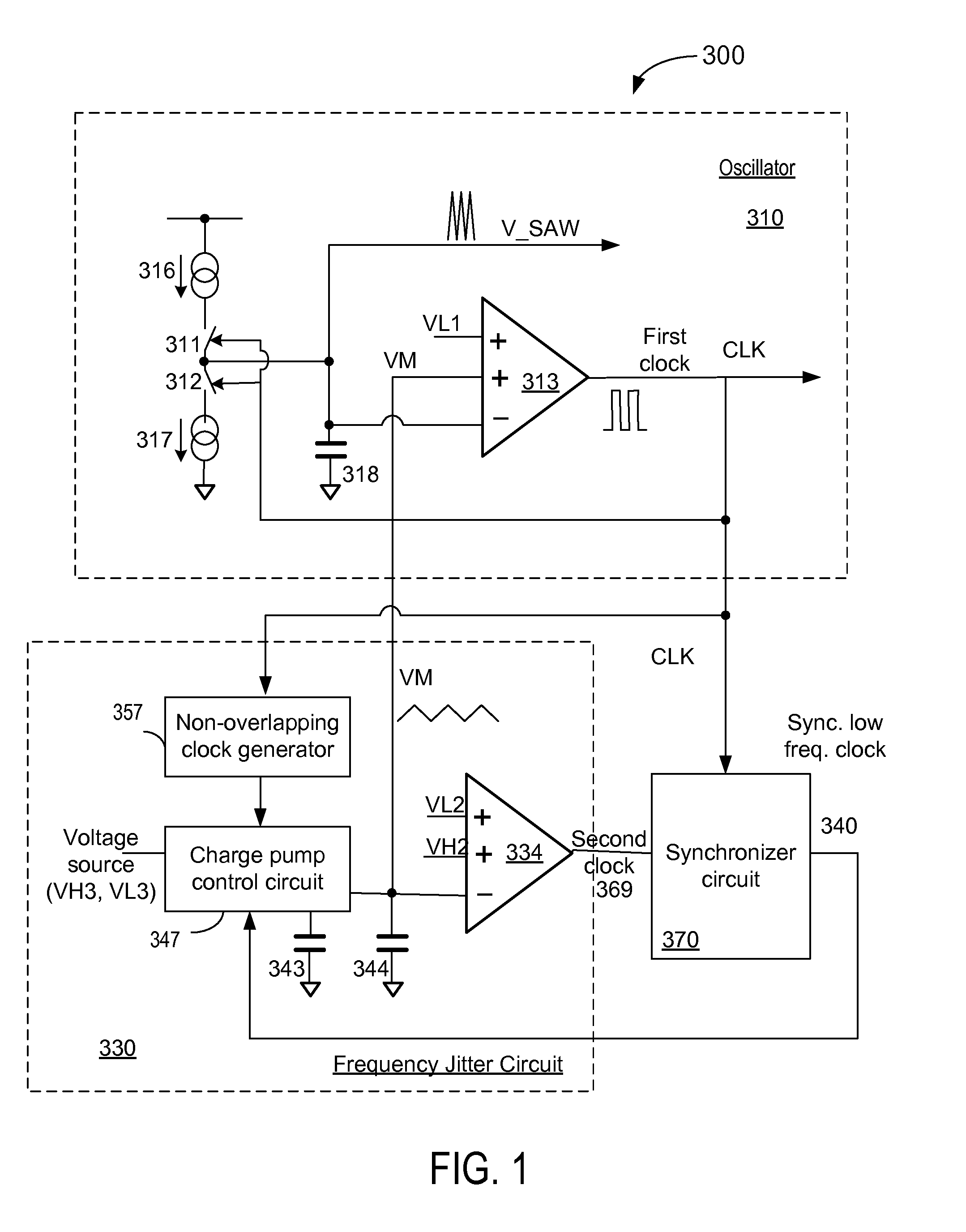
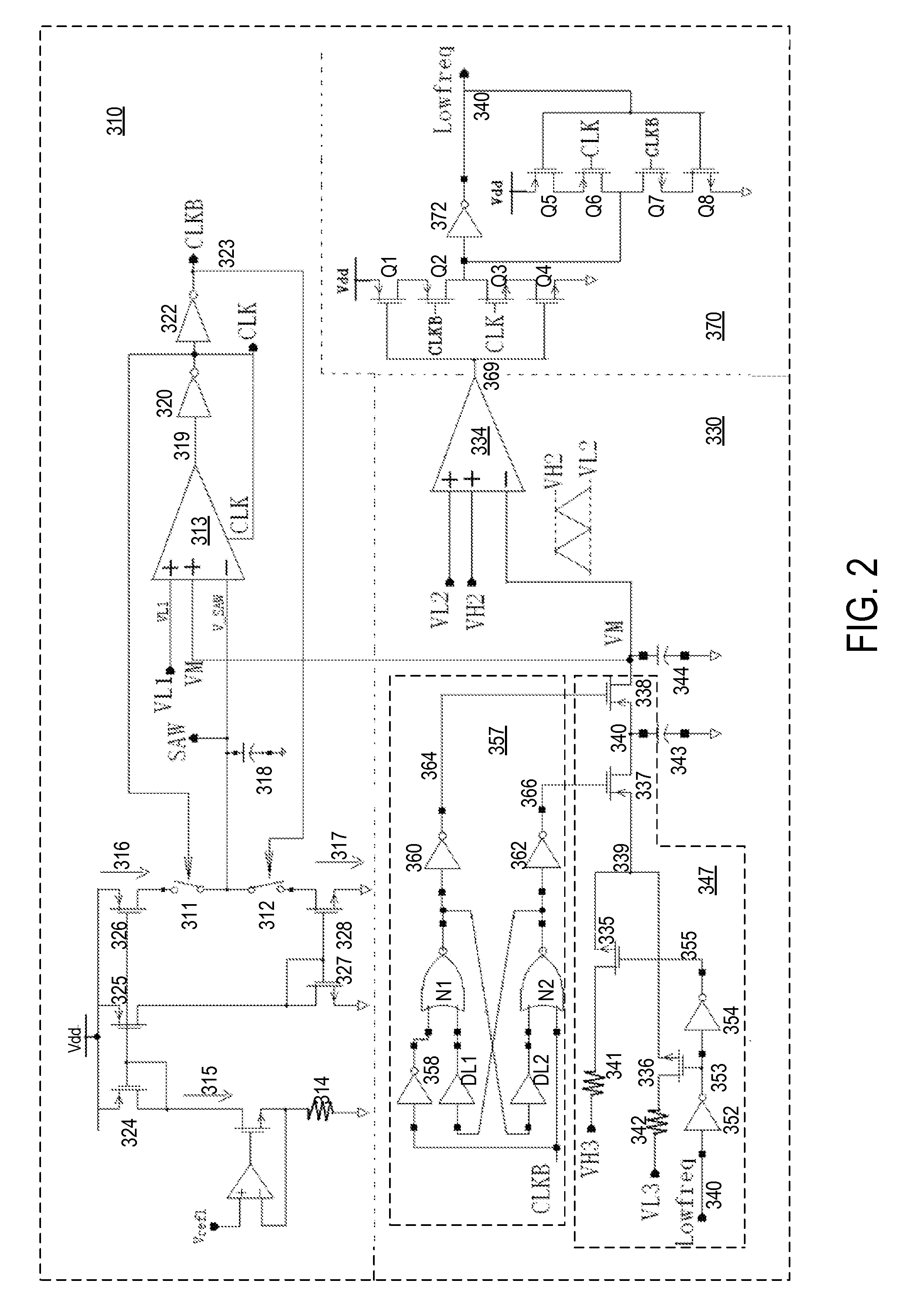
[0048]FIG. 1 is a block diagram of an oscillator circuit 300 according to one embodiment of the present invention. This diagram is merely an example, which should not unduly limit the scope of the claims herein. Oscillator circuit 300 includes an oscillator 310, a frequency jitter circuit 330 that provides a time-varying voltage VM to oscillator 310, and a synchronizer circuit 370. Oscillator 310 includes a first comparator 313 having a first positive input terminal coupled to a voltage VL1, a second positive input terminal coupled to voltage VM provided by frequency jitter circuit 330, a negative input terminal coupled to a capacitor 318, and an output terminal which provides a first clock signal CLK. Capacitor 318 is charged by a source current 316 and discharged by a sink current 317 through a respective source switch 311 and sink switch 312 in step with first clock CLK. Capacitor 318 thus generates a voltage V_SAW swinging in step with first clock CLK. Thus, a change in first cl...


PUM


Abstract

Method and apparatus for adding jitter to an oscillator for reducing EMI are disclosed An oscillator circuit includes an oscillator configured to generate a first clock having a first frequency and a frequency jitter circuit including a charge pump configured to charge and discharge first and second capacitors repeatedly for obtaining a time-varying voltage having a second frequency. The time-varying voltage is coupled to the oscillator to vary the first frequency within a frequency range. The charge pump includes a first switch for coupling the first capacitor to a voltage source and a second switch for coupling the first capacitor to the second capacitor. A charge transfer between the first and second capacitors is configured to provide the time-varying voltage.

Description

CROSS-REFERENCES TO RELATED APPLICATIONS[0001]This application claims priority to Chinese Patent Application No. 200910132657.2 filed Mar. 30, 2009, which is commonly owned and incorporated herein by reference.BACKGROUND OF THE INVENTION[0002]The present invention relates to switching mode power supplies. More particularly, the invention provides methods and apparatuses for reducing electromagnetic interference (EMI) of switching mode power supplies.[0003]Many electronic components require clean DC power sources that may obtained from other DC or AC power sources using switching mode power regulation systems. Generally, transformer may be used to convert a DC power source to the desired DC power. In order to obtain a small size of transformers, the switching frequency has to be high relative to the alternating current (AC) power line. However, the relative high switching frequency can be coupled back to the AC power line and interfere with the operation of other radio frequency oper...

Claims


Application Information

Patent Timeline
IPC IPC(8): H02M7/5383H03L7/06
CPCH02M1/44H03K4/501H03K3/84
Inventor YING, ZHENGXU, HUANG ZHANG
Owner BCD SHANGHAI MICRO ELECTRONICS CO LTD
Why Eureka
Try Eureka