Selective deposition of metal-containing cap layers for semiconductor devices

a technology of metal-containing cap layer and semiconductor device, which is applied in the direction of semiconductor/solid-state device manufacturing, basic electric elements, electric apparatus, etc., can solve the problems of affecting the acceptance of this complex process, em and sm have fast become critical challenges, and the defects that can destroy an integrated circuit, etc., to improve the effect of electromigration and stress migration

Active Publication Date: 2010-09-30
TOKYO ELECTRON LTD
View PDF28 Cites 134 Cited by
  • Summary
  • Abstract
  • Description
  • Claims
  • Application Information

AI Technical Summary

Benefits of technology

[0006]Embodiments of the invention provide methods for manufacturing semiconductor devices by integrating metal-containing cap layers into Cu metallization to improve electromigration and stress migration in bulk Cu metal layers. The methods provide improved selective deposition of metal-containing cap layers on patterned substrates containing metal surfaces and dielectric layer surfaces by modifying the dielectric layer surfaces prior to depositing the metal-containing cap layers selectively on the metal surfaces.

Problems solved by technology

The use of Cu metal in multilayer metallization schemes for manufacturing integrated circuits has created several problems that require solutions.
For example, high mobility of Cu atoms in dielectric materials and silicon(Si) can result in migration of Cu atoms into those materials, thereby forming electrical defects that can destroy an integrated circuit.
Because electromigration (EM) and stress migration (SM) lifetimes are inversely proportional to current density, EM and SM have fast become critical challenges.
However, maintaining acceptable deposition selectivity on bulk Cu metal, especially for tight pitch Cu wiring, and maintaining good film uniformity, has affected acceptance of this complex process.
Furthermore, wet process steps using acidic solution may be detrimental to the use of CoWP.

Method used


Image

  • Selective deposition of metal-containing cap layers for semiconductor devices
  • Selective deposition of metal-containing cap layers for semiconductor devices
  • Selective deposition of metal-containing cap layers for semiconductor devices

Examples


Embodiment Construction

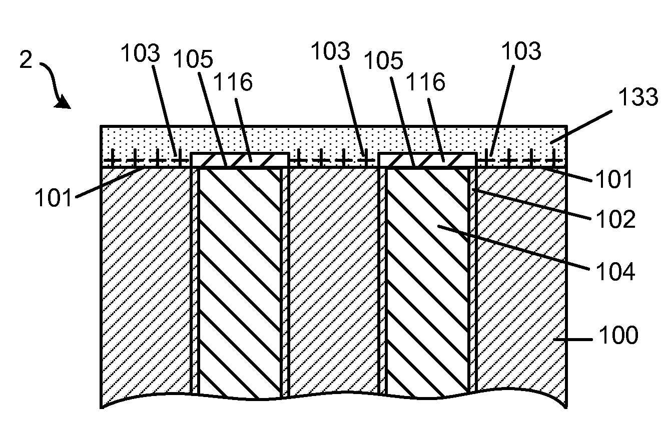
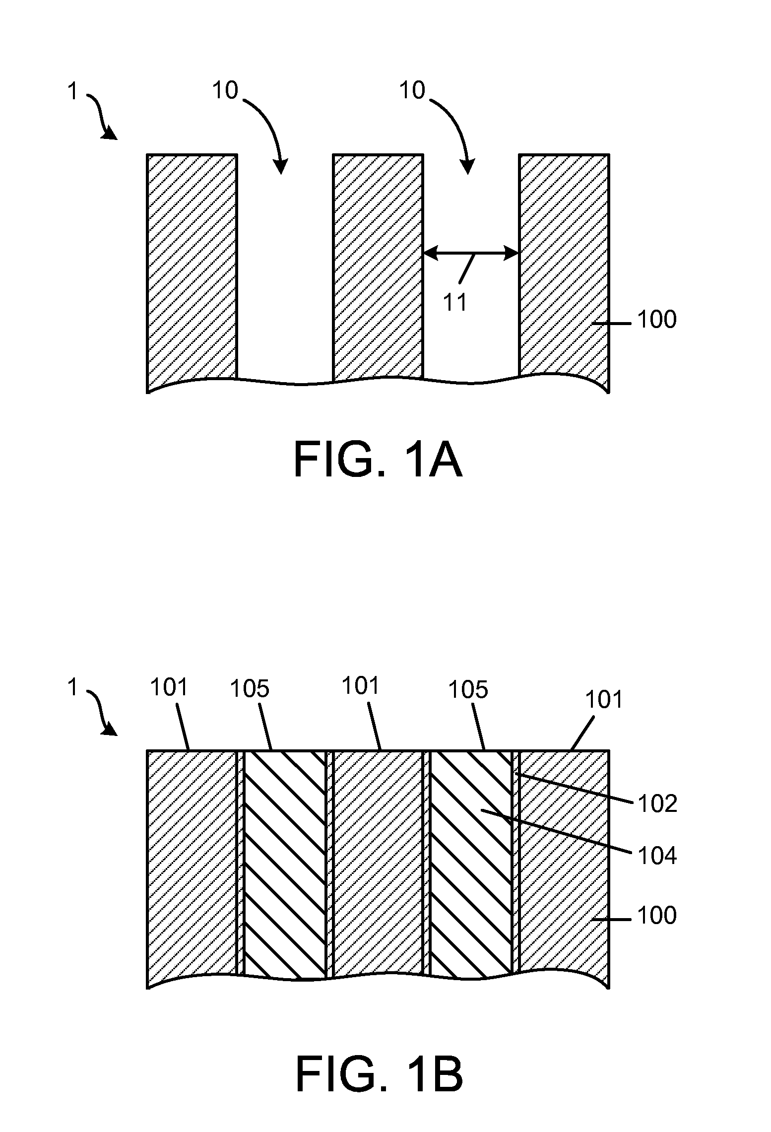
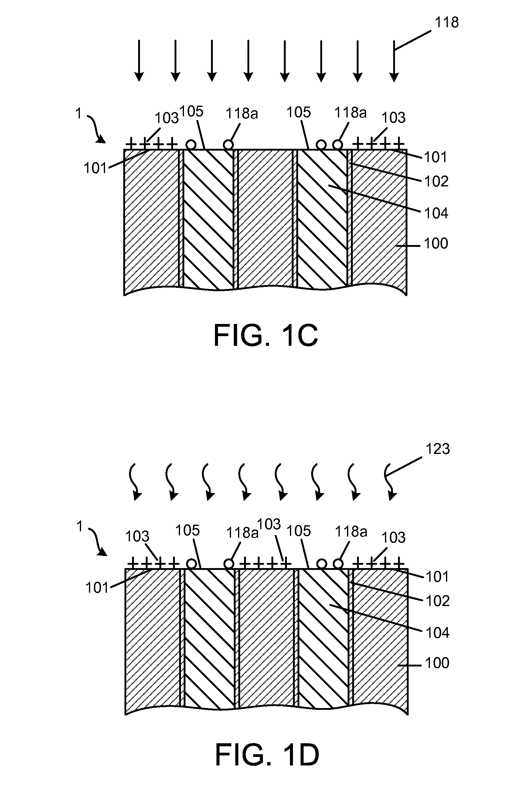
[0019]Embodiments of the invention provide methods for integrating metal-containing cap layers into Cu metallization of semiconductor devices to improve electromigration and stress migration in the devices. Although the presence of metal-containing cap layers on metal surfaces (e.g., Cu surfaces or tungsten (W) surfaces) in semiconductor devices is extremely beneficial to the electromigration and stress migration properties of the Cu metallization layers, the presence of even trace amounts of additional metal-containing material on dielectric layer surfaces adjacent the metal layers is detrimental to the various electrical properties of a semiconductor device.

[0020]As the minimum feature sizes of semiconductor devices decrease and the thickness of the dielectric layers between adjacent metal layers decreases, electromigration and stress migration problems become increasingly more serious. In one example, a 32 nm minimum feature size device generation may utilize only about 45-50 nm ...


PUM

PropertyMeasurementUnit
dielectric thicknessaaaaaaaaaa
widthaaaaaaaaaa

Abstract

A method for integrating metal-containing cap layers into copper (Cu) metallization of semiconductor devices. In one embodiment, the method includes providing a patterned substrate containing metal surfaces and dielectric layer surfaces, and modifying the dielectric layer surfaces by exposure to a reactant gas containing a hydrophobic functional group, where the modifying substitutes a hydrophilic functional group in the dielectric layer surfaces with a hydrophobic functional group. The method further includes depositing metal-containing cap layers selectively on the metal surfaces by exposing the modified dielectric layer surfaces and the metal surfaces to a deposition gas containing metal-containing precursor vapor.

Description

FIELD OF THE INVENTION[0001]The present invention relates to semiconductor processing and semiconductor devices, and more particularly, to methods for integrating metal-containing cap layers into copper (Cu) metallization of semiconductor devices to improve electromigration (EM) and stress migration (SM) in bulk Cu metal.BACKGROUND OF THE INVENTION[0002]An integrated circuit contains various semiconductor devices and a plurality of conducting metal paths that provide electrical power to the semiconductor devices and allow these semiconductor devices to share and exchange information. Within the integrated circuit, metal layers are stacked on top of one another using intermetal or interlayer dielectric layers that insulate the metal layers from each other. Normally, each metal layer must form an electrical contact to at least one additional metal layer. Such electrical contact is achieved by etching a hole (i.e., a via) in the interlayer dielectric that separates the metal layers, an...

Claims


Application Information

Patent Timeline
Patent Type & Authority Applications(United States)
IPC IPC(8): H01L21/768H01L21/3205
CPCH01L21/02063H01L21/02074H01L21/3105H01L21/76814H01L21/76826H01L21/76883H01L21/76846H01L21/76849H01L21/76856H01L21/76859H01L21/76828
Inventor ISHIZAKA, TADAHIROMIZUNO, SHIGERUHOSHINO, SATOHIKONAGAI, HIROYUKICHIBA, YUKICERIO, JR., FRANK M.
Owner TOKYO ELECTRON LTD
Why Eureka
Try Eureka