Lighting device

a technology of light source and backlight, which is applied in the direction of lighting and heating apparatus, instruments, optical elements, etc., can solve the problems of difficult positioning of light source, difficult to dissipate heat, and undesirable characteristics of such a backlight, etc., and achieves the effect of increasing the light emission angle, increasing the light intensity, and increasing the area

Active Publication Date: 2010-10-07
SHENZHEN JUFEI OPTOELECTRONICS
View PDF12 Cites 47 Cited by
  • Summary
  • Abstract
  • Description
  • Claims
  • Application Information

AI Technical Summary

Benefits of technology

[0023]According to the lighting device of the present invention, the characteristic of increasing the emitted light intensity sharply with increasing light emission angle is obtained, which makes it possible to illuminate a larger area with a nearly uniform illuminance. Therefore, when the lighting device of the present invention is used in a backlight of a liquid crystal display it is expected to contribute to a reduction in the thickness of the display.

Problems solved by technology

As the screen size increases, the required light quantity density increases, which makes it more difficult to position the light source, and the heat generation density also increases, which makes it more difficult to dissipate the heat.
Since the LED light sources used for a direct type backlight are required to have a characteristic of illuminating a largest possible area uniformly with a smallest possible number of LED light sources, the characteristic as mentioned above is not desirable for such a backlight.
It is, however, not easy to obtain the characteristic of increasing the emitted light intensity sharply with increasing angle as shown in FIG. 4.
In particular, the difficulty of obtaining the above-mentioned characteristic increases further if a LED of limited size and an encapsulating resin of limited size are used.

Method used


Image

  • Lighting device
  • Lighting device
  • Lighting device

Examples


Embodiment Construction

[0028]Hereinafter, embodiments of the present invention will be described with reference to the accompanying drawings.

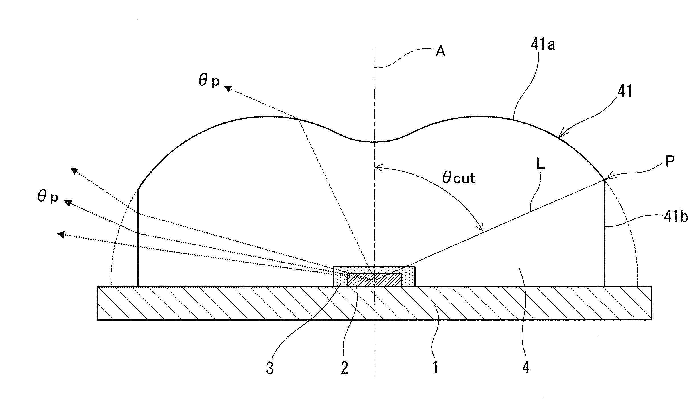
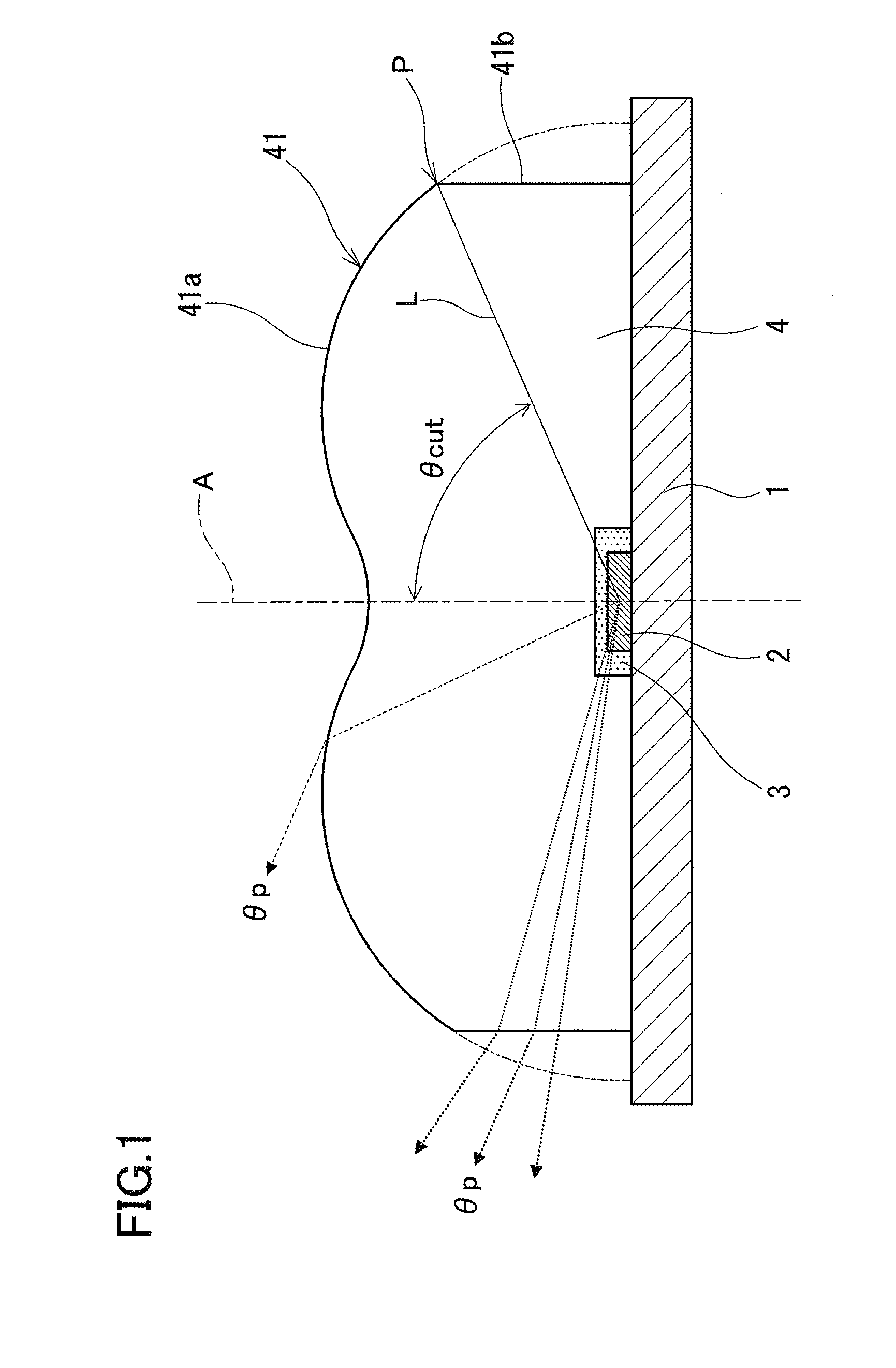
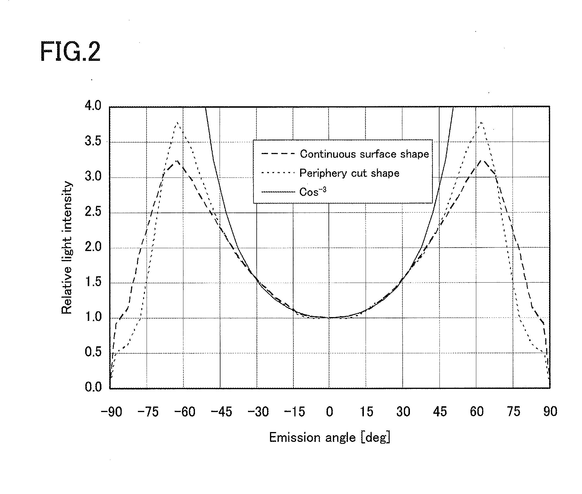
[0029]FIG. 1 is a cross-sectional view of a lighting device (surface illumination device) according to one embodiment of the present invention. This lighting device includes a mounting substrate 1, a LED element 2 mounted on the mounting substrate 1, and a lens 4 disposed on the mounting substrate 1 so as to cover the LED element 2.

[0030]In the present embodiment, a blue LED chip is used as the LED element 2. A phosphor layer 3 for converting blue light into yellow light is provided around the LED element 2 so as to encompass the LED element 2 from the side opposite to the mounting substrate 1.

[0031]Furthermore, in the present embodiment, the LED element 2 and the phosphor layer 3 are encapsulated with transparent resin, and this transparent resin forms a lens 4. When the encapsulation with the transparent resin is performed, the surface of the transparent resin, whi...


PUM


Abstract

A lighting device includes a substrate, a LED element, and a lens. A light exit surface of the lens includes a first light exit surface and a second light exit surface. A curve obtained by cutting the light exit surface by a plane including the optical axis has, on a boundary between the first light exit surface and the second light exit surface, a change point at which a rate of inclination decreases discontinuously. An angle between the optical axis and a line segment connecting the change point and a light emission center of the LED element is approximately equal to an emission angle with the highest light intensity, among emission angles, when light rays emitted from the light exit surface are sorted by respective emission angles.

Description

BACKGROUND OF THE INVENTION[0001]1. Field of the Invention[0002]The present invention relates to a lighting device to be used suitably in, for example, a backlight of a liquid crystal display.[0003]2. Description of Related Art[0004]In recent years, with a remarkably enhanced efficiency and reduced cost of light emitting diodes (LEDs), LEDs have replaced conventional fluorescent tubes as dominant light sources for backlights of small and medium-sized liquid crystal displays, and further are gaining widespread use as light sources for large-screen liquid crystal displays or for general illumination.[0005]In large-screen liquid crystal displays like liquid crystal TVs, direct type backlights have been used widely instead of edge light type backlights, which are commonly used in small and medium-sized liquid crystal displays. This is because such edge light type backlights have the following disadvantages.[0006]An edge light type backlight is configured such that a light source is disp...

Claims


Application Information

Patent Timeline
Patent Type & Authority Applications(United States)
IPC IPC(8): F21V5/04
CPCG02F1/133603G02B19/0061G02B19/0014H01L33/54
Inventor YAMAGUCHI, HIROSHI
Owner SHENZHEN JUFEI OPTOELECTRONICS
Why Eureka
Try Eureka