Thin film type solar cell and method for manufacturing the same
- Summary
- Abstract
- Description
- Claims
- Application Information
AI Technical Summary
Benefits of technology
Problems solved by technology
Method used
Image

Examples
first embodiment
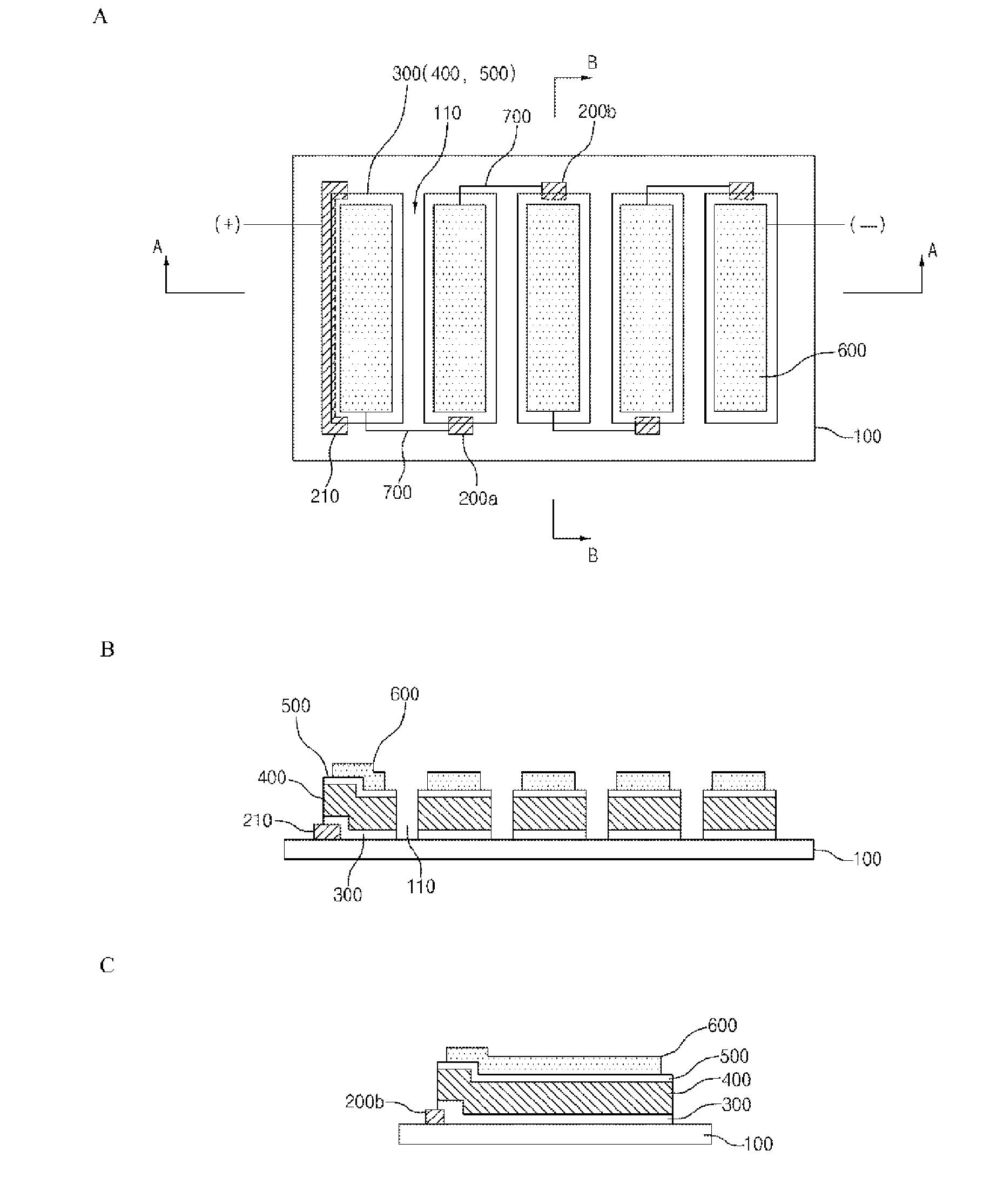
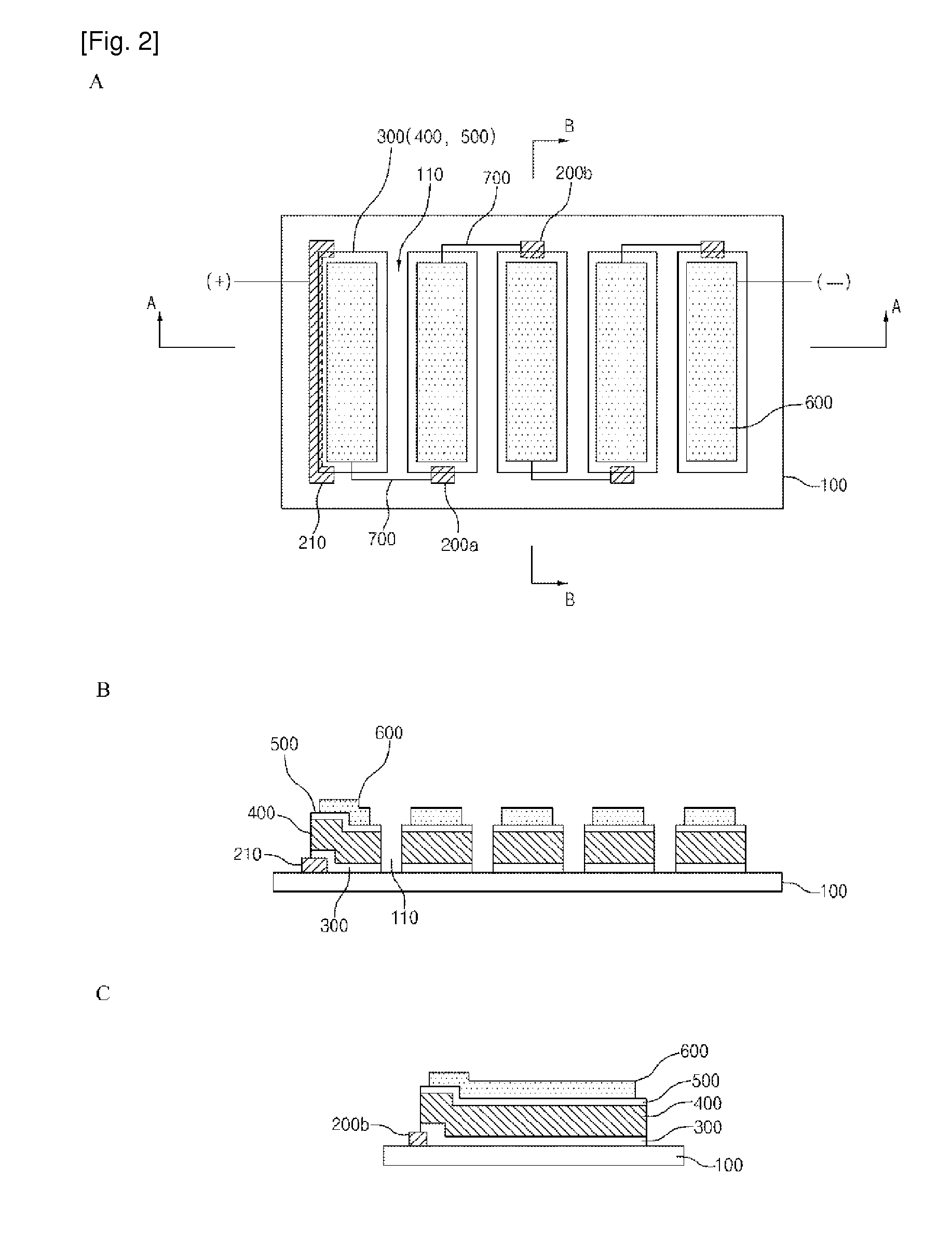
[0060]FIG. 2A is a plan view illustrating a thin film type solar cell according to the first embodiment of the present invention, FIG. 2B is a cross section view along A-A of FIG. 2A, and FIG. 2C is a cross section view along B-B of FIG. 2A.
[0061]As shown in FIGS. 2A to 2C, the thin film type solar cell according to the first embodiment of the present invention includes a substrate 100, auxiliary electrodes 200a and 200b, front electrodes 300, semiconductor layer patterns 400, transparent conductive layer patterns 500, and rear electrodes 600.
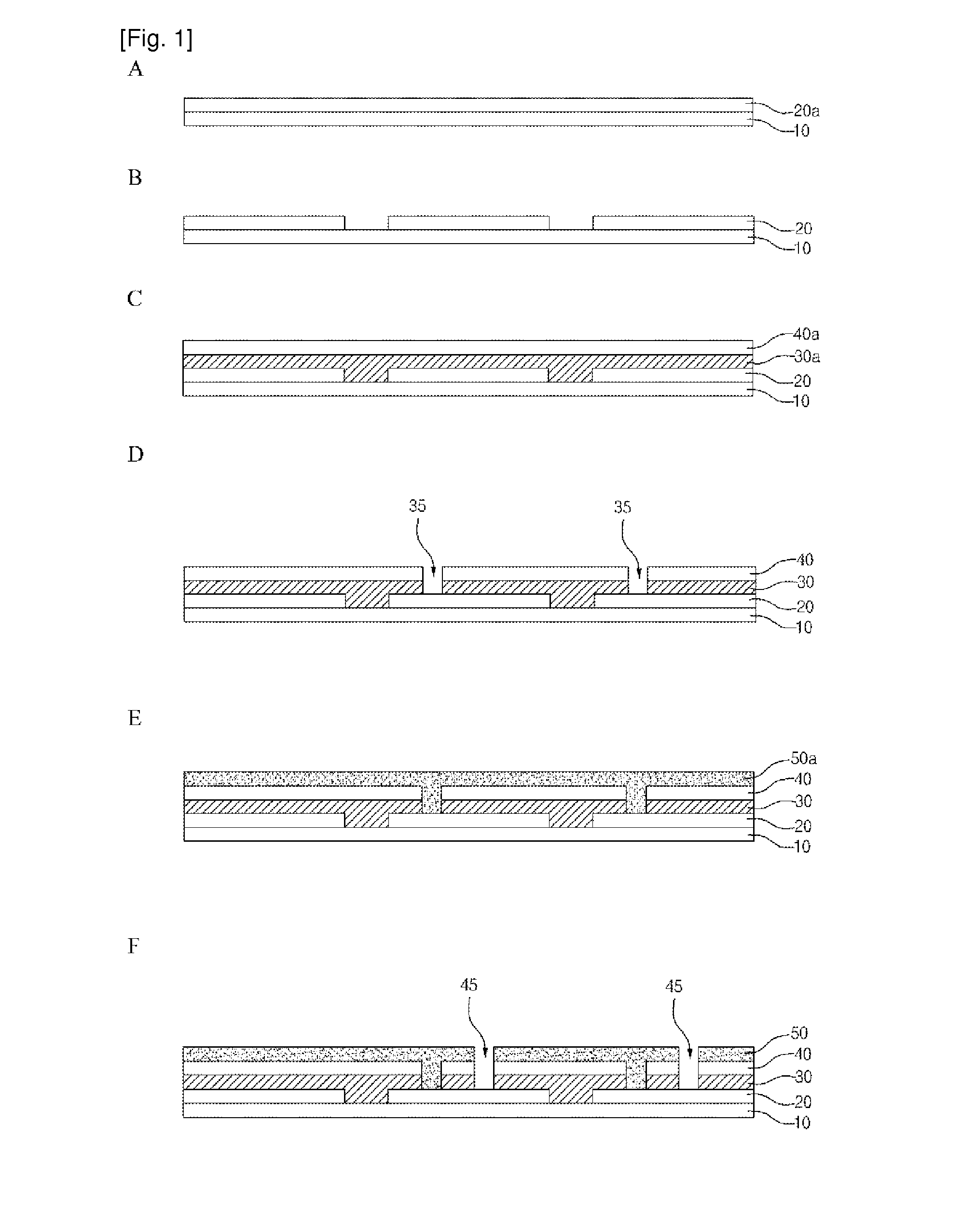
[0062]At this time, the substrate 100 may be formed of glass or transparent plastic. Also, a plurality of separating parts 110 are interposed between each of the front electrodes 300, the semiconductor layer patterns 400, the transparent conductive layer patterns 500, and the rear electrodes 600, whereby they are arranged at fixed intervals owing to the interposed separating parts 110. That is, the solar cell according to the first embodiment o...
second embodiment
[0083]FIG. 3A is a plan view illustrating a thin film type solar cell according to the second embodiment of the present invention, FIG. 3B is a cross section view along A-A of FIG. 3A, and FIG. 3C is a cross section view along B-B of FIG. 3A.
[0084]Except for separating parts 110a and 110b for dividing a solar cell into a plurality of unit cells, the thin film type solar cell according to the second embodiment of the present invention is identical in structure to the thin film type solar cell according to the first embodiment of the present invention.
[0085]The thin film type solar cell according to the second embodiment of the present invention is comprised of a plurality of first straight-line grooves 110a arranged at a first direction (for example, a short-side direction of substrate in FIG. 3A), and a second straight-line groove 110b arranged at a second direction (for example, a long-side direction of substrate in FIG. 3A), wherein the first direction is perpendicular to the seco...
third embodiment
[0089]FIG. 4A is a plan view illustrating a thin film type solar cell according to the third embodiment of the present invention, FIG. 4B is a cross section view along A-A of FIG. 4A, and FIG. 4C is a cross section view along B-B of FIG. 4A.
[0090]Except that an insulating layer pattern 800 is additionally formed under the semiconductor layer pattern 400, the thin film type solar cell according to the third embodiment of the present invention is identical in structure to the thin film type solar cell according to the first embodiment of the present invention.
[0091]According as the insulating layer pattern 800 is formed under the semiconductor layer pattern 400, the entire size of the semiconductor layer pattern 400 is increased so that the solar cell efficiency is improved.
[0092]That is, in comparison to the case of omitting the insulating layer pattern 800, the case of forming the insulating layer pattern 800 can realize higher solar cell efficiency owing to the increased entire siz...
PUM
 Abstract
Description
Claims
Application Information
 - R&D Engineer
- R&D Manager
- IP Professional
- Industry Leading Data Capabilities
- Powerful AI technology
- Patent DNA Extraction
Browse by: Latest US Patents, China's latest patents, Technical Efficacy Thesaurus, Application Domain, Technology Topic.
© 2024 PatSnap. All rights reserved.Legal|Privacy policy|Modern Slavery Act Transparency Statement|Sitemap