Method Of Efficient Coupling Of Light From Single-Photon Emitter To Guided Radiation Localized To Sub-Wavelength Dimensions On Conducting Nanowires

a single-photon emitter and guided radiation technology, applied in the direction of optical radiation measurement, luminescent dosimeters, instruments, etc., can solve the problems of controlling the interaction between single photons and individual optical emitters, and achieve the effects of improving the efficiency of single-photon emitter interaction

Inactive Publication Date: 2010-10-14
PRESIDENT & FELLOWS OF HARVARD COLLEGE +1
View PDF4 Cites 13 Cited by
  • Summary
  • Abstract
  • Description
  • Claims
  • Application Information

AI Technical Summary

Benefits of technology

[0010]The present invention extends these developments in two principal directions. First, the present invention results simultaneously in significant enhancement of SP emission and efficient collection into guided modes propagating along a well-defined direction. Second, it establishes direct coupling between individual emitters and individual, quantized SPs. It thus bridges the fields of nanoscale plasmonics and quantum optics, and opens up the possibility of using quantum optical techniques to achieve new levels of control over the interaction of single SPs and to realize novel quantum plasmonic devices. In conventional setups, the benefits of using smaller wires must be balanced against poor out-coupling to free-space modes. However, this tradeoff can be circumvented by the present invention by using optimized geometries (e.g., SPs on conducting nanotips) and evanescent out-coupling to mode-matched optical fibers. The excellent coupling expected from these integrated systems can be uniquely used, e.g., for efficient single-photon sources, high resolution microscopy and sensing, or long-range quantum bit coupling. See, Klimov, V. V., Ducloy, M., Letokhov, V. S., “A model of an apertureless scanning microscope with a prolate nanospheroid as a tip and an excited molecule as an object,”Chem. Phys. Lett. 358,192 (2002). Furthermore, in such systems an individual emitter can be made optically opaque to incident, localized single SPs, which can be used to produce large optical nonlinearities for realization of single photon switches and photonic transistors. See, Chang, D. E., Sørensen, A. S., Demler, E. A., Lukin, M. D. “A single-photon transistor using nano-scale surface plasmons”, quant-ph / 0706.4335. Beyond these specific applications, the ability to create and control individual quanta of radiation with sub-wavelength localization may open up intriguing possibilities on the interface of several areas of optics and electronics.
[0015]In another preferred embodiment, the present invention is a method for efficient creation of single photons for quantum cryptography. The method comprises the step of creating strong coupling between single optical plasmons guided on nanowires and single emitters to form an efficient quantum interface between photonic and matter quantum bits.

Problems solved by technology

Control over the interaction between single photons and individual optical emitters is an outstanding problem in quantum science and engineering.

Method used


Image

  • Method Of Efficient Coupling Of Light From Single-Photon Emitter To Guided Radiation Localized To Sub-Wavelength Dimensions On Conducting Nanowires
  • Method Of Efficient Coupling Of Light From Single-Photon Emitter To Guided Radiation Localized To Sub-Wavelength Dimensions On Conducting Nanowires
  • Method Of Efficient Coupling Of Light From Single-Photon Emitter To Guided Radiation Localized To Sub-Wavelength Dimensions On Conducting Nanowires

Examples


Embodiment Construction

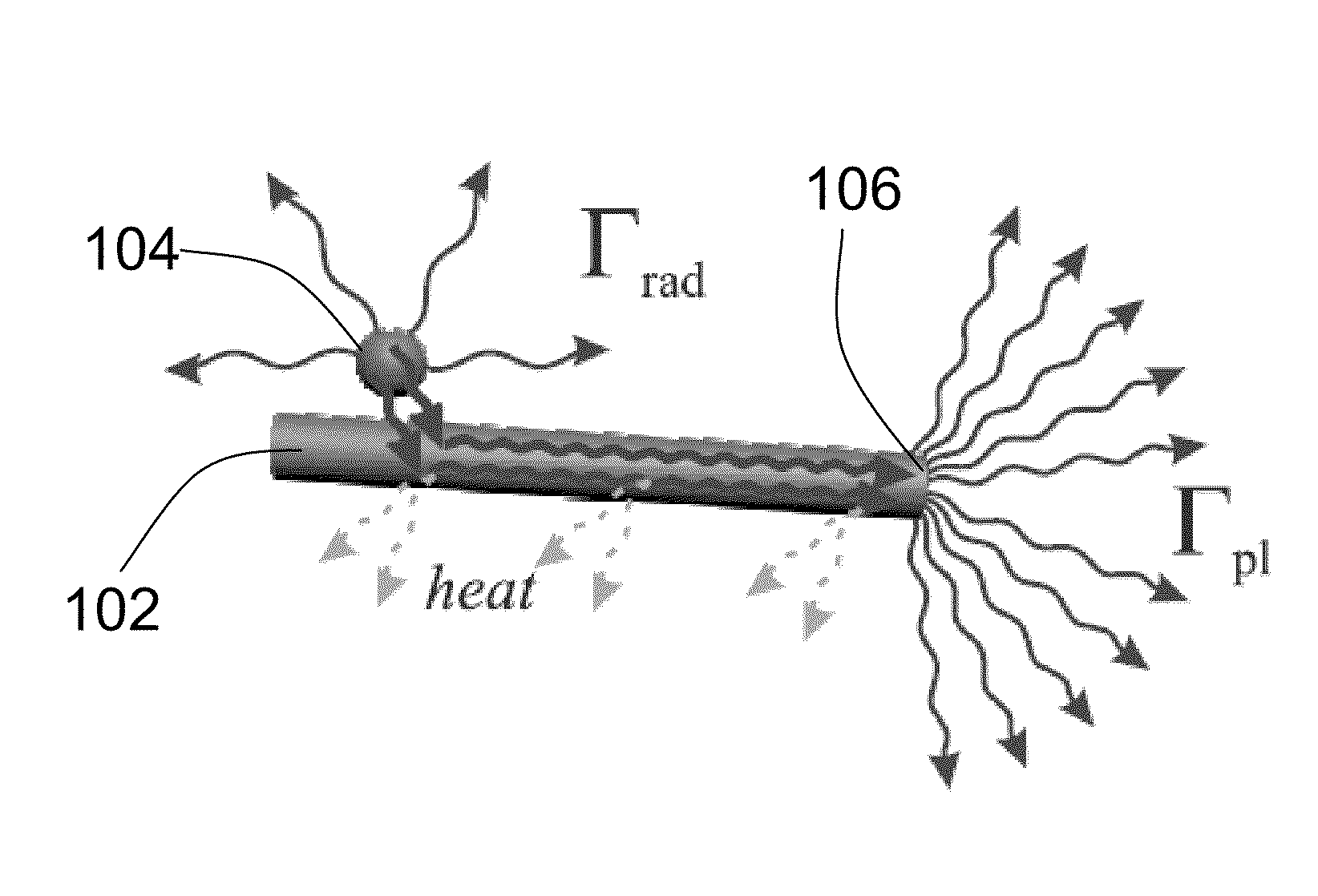
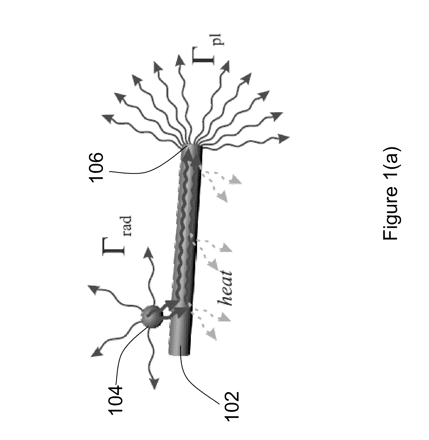
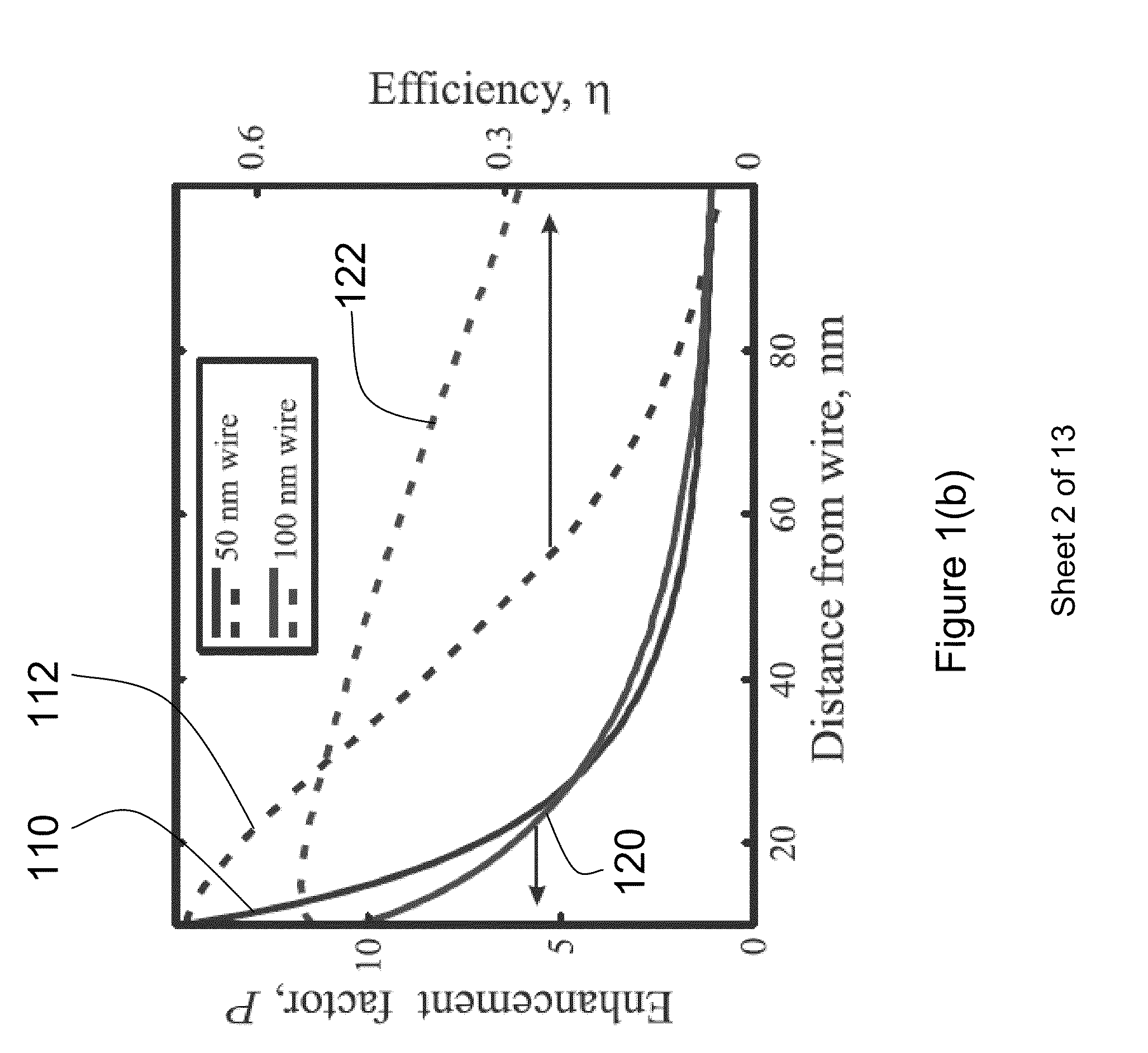
[0035]The present disclosure demonstrates a cavity free, broadband approach for engineering photon emitter interactions via sub-wavelength confinement of optical fields near metallic nanostructures. For background, see Chang, D. E., Sørensen, A. S., Hemmer, P. R., Lukin, M. D., “Quantum Optics with Surface Plasmons,”Phys. Rev. Lett. 97, 053002 (2006); Atwater, H. A., “The promise of plasmonics,”Scientific American 296(4), 56 (2007); Genet, C., Ebbesen, T. W., “Light in tiny holes,”Nature 445, 39 (2007). When a single CdSe quantum dot (QD) is optically excited in close proximity to a silver nanowire (NW), emission from the QD couples directly to guided surface plasmons in the NW, causing the wire's ends to light up. Sanders, A. W., Routenberg, D. A., Wiley, B. J., Xia, Y., Dufresne, E. R., Reed, M. A., “Observation of Plasmon Propagation, Redirection, and FanOut in Silver Nanowires,”Nano Lett. 6(8), 1822 (2006); Ditlbacher, H., Hohenau, A., Wagner, D., Kreibig, U., Rogers, M., Hofer ...


PUM


Abstract

A cavity free, broadband approach for engineering photon emitter interactions via sub-wavelength confinement of optical fields near metallic nanostructures. When a single CdSe quantum dot (QD) is optically excited in close proximity to a silver nanowire (NW), emission from the QD couples directly to guided surface plasmons in the NW, causing the wire's ends to light up. Nonclassical photon correlations between the emission from the QD and the ends of the NW demonstrate that the latter stems from the generation of single, quantized plasmons. Results from a large number of devices show that the efficient coupling is accompanied by more than 2.5-fold enhancement of the QD spontaneous emission, in a good agreement with theoretical predictions.

Description

CROSS-REFERENCE TO RELATED APPLICATIONS[0001]The present application claims the benefit of the filing date of U.S. Provisional Patent Application Ser. No. 60 / 973,288 filed on Sep. 18, 2007 and entitled “Method Of Efficient Coupling Of Light From Single-Photon Emitter To Guided Radiation Localized To Sub-Wavelength Dimensions On Conducting Nanowires.”[0002]The above-referenced provisional patent application is hereby incorporated by reference herein in its entirety.STATEMENT REGARDING FEDERALLY SPONSORED RESEARCH OR DEVELOPMENT[0003]The present invention may have been developed with funding from one or more of the following government contracts: DARPA FA9550-04-1-0455, NSF (Career) PHY 0134776, NSF (NIRT) ECCS-0708905, NSF (CUA) PHY 0551153, DTO ARO STIC W911NF-05-1-0476, and NSF (NIRT) ECS-0210426.BACKGROUND OF THE INVENTION[0004]1. Field of the Invention[0005]The present invention relates to a broadband approach for engineering photon-emitter interactions via sub-wavelength confine...

Claims


Application Information

Patent Timeline
Patent Type & Authority Applications(United States)
IPC IPC(8): H01L29/66G02B6/00H01L31/0232F21V8/00G02B6/26
CPCB82Y20/00G02B6/1226G02B6/107
Inventor LUKIN, MIKHAIL D.ZIBROV, ALEXANDER S.AKIMOV, ALEXEY V.HEMMER, PHILIP R.PARK, HONGKUNMUKHERJEE, ARYESHCHANG, DARRICK E.YU, CHUN LIANG
Owner PRESIDENT & FELLOWS OF HARVARD COLLEGE
Why Eureka
Try Eureka