
Transparent electroconductive laminate and transparent touch panel

Inactive Publication Date: 2010-10-14
TEIJIN LTD
View PDF4 Cites 26 Cited by
  • Summary
  • Abstract
  • Description
  • Claims
  • Application Information

AI Technical Summary

Benefits of technology

[0037]According to the present invention, a transparent touch panel having improved writing durability, particularly in the edge region (edge-pressing durability), without deteriorating the optical properties and environmental reliability required for a transparent touch panel, is provided. Further, a transparent electroconductive laminate suitable for such a transparent touch panel is provided.

Problems solved by technology

In any of these methods, two transparent polymer films are laminated through an adhesive or a transparent resin layer, and this causes a problem that the production process is complicated and the production efficiency is low, although a writing durability is improved.
Moreover, when a large transparent touch panel exceeding 10 inches is produced, the transparent electroconductive laminate is disadvantageously flexed due to structurally low rigidity.
However, for example, a transparent electroconductive laminate using an electroconductive polymer material as the transparent electrode has a problem that contact resistance obtained when transparent electroconductive layers are in contact with each other in the transparent touch panel is large, and therefore the transparent touch panel does not work, or a problem that transmittance and environmental reliability cannot be ensured.
Therefore, when a polyethylene terephthalate generally used as a movable electrode substrate of a transparent touch panel is used as the polymer film, oligomer components are disadvantageously mitigated from the polymer film after a heat treatment and the like.
Furthermore, since the properties of the transparent electroconductive layer are not specified, there is a problem that when such a transparent electroconductive laminate is used for a transparent touch panel, writing durability necessary for a transparent touch panel cannot be ensured.

Method used


Image

  • Transparent electroconductive laminate and transparent touch panel
  • Transparent electroconductive laminate and transparent touch panel
  • Transparent electroconductive laminate and transparent touch panel

Examples


examples

[0204]The present invention is described below by referring to specific working examples, but the present invention is not limited thereto. In Examples below, the linearity measuring method, the edge-pressing durability test method, the total light transmittance measuring method, and the environmental reliability evaluating method are as follows.

[0205]A direct current voltage of 5 V is applied between parallel electrodes on a movable electrode substrate or a fixed electrode substrate, and a voltage is measured at intervals of 5 mm in the direction perpendicular to the parallel electrodes. Assuming that the voltage at the measurement start position A is EA, the voltage at the measurement end position B is EB, the actually measured voltage at a distance X from A is EX, the theoretical value is ET, and the linearity is L, the linearity is determined according to following formula:

ET=(EB−EA)×X / (B−A)+EA

L(%)=(|ET−EX|) / (EB−EA)×100

[0206]A writing durability test is performed by linearly mo...

examples i-1 to i-6

, and Comparative Examples I-1 to I-20

[0215]In the following Examples I-1 to I-6, and Comparative Examples I-1 to I-20, the embodiment of the present invention which cases the transparent electroconductive layer-2 containing an ionizing radiation-curable resin and a fine particle A of electroconductive metal oxide or metal is studied.

example i-1

Formation of Hardcoat Layer

[0216]On one surface of a 188 μm-thick polyethylene terephthalate film (“OFW”, produced by Teijin DuPont Films), a hardcoat layer having a film thickness of 4 μm was formed by using an ultraviolet-curable polyfunctional acrylate resin coating material.

(Formation of Cured Resin Layer)

[0217]100 Parts by weight of tetrafunctional acrylate “Aronix” M400 (produced by Toagosei Co., Ltd.), 5 parts by weight of “Irgacure” 184 (produced by Ciba Specialty Chemicals Inc.), and 0.7 parts by weight of “Hipresica” (particle of 3.0 μm (grade: N3N), produced by Ube-Nitto Kasei Co., Ltd.) were dissolved in a 1:1 mixed solvent of isopropyl alcohol and 1-methoxy-2-propanol. Thereafter, to the obtained mixture, an MgF2 ultrafine particle (produced by C.I. Kasei Co., Ltd. (a 20 wt % liquid dispersion in an ethyl alcohol / n-butyl alcohol mixed solvent)) having an average primary particle diameter of 30 nm was added such that a solid content is 5 parts by weight per 100 parts by ...


PUM


Abstract

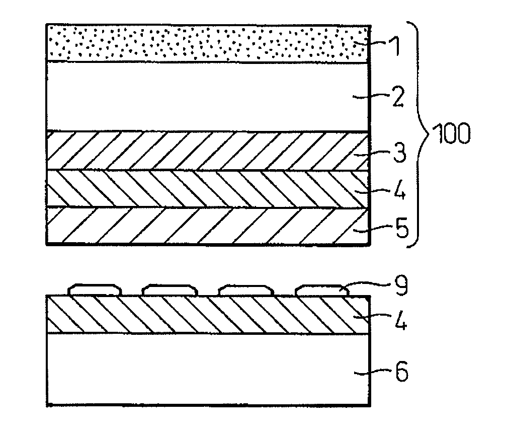
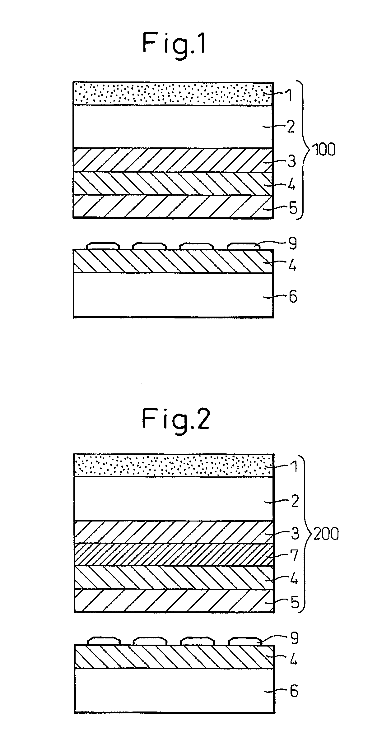
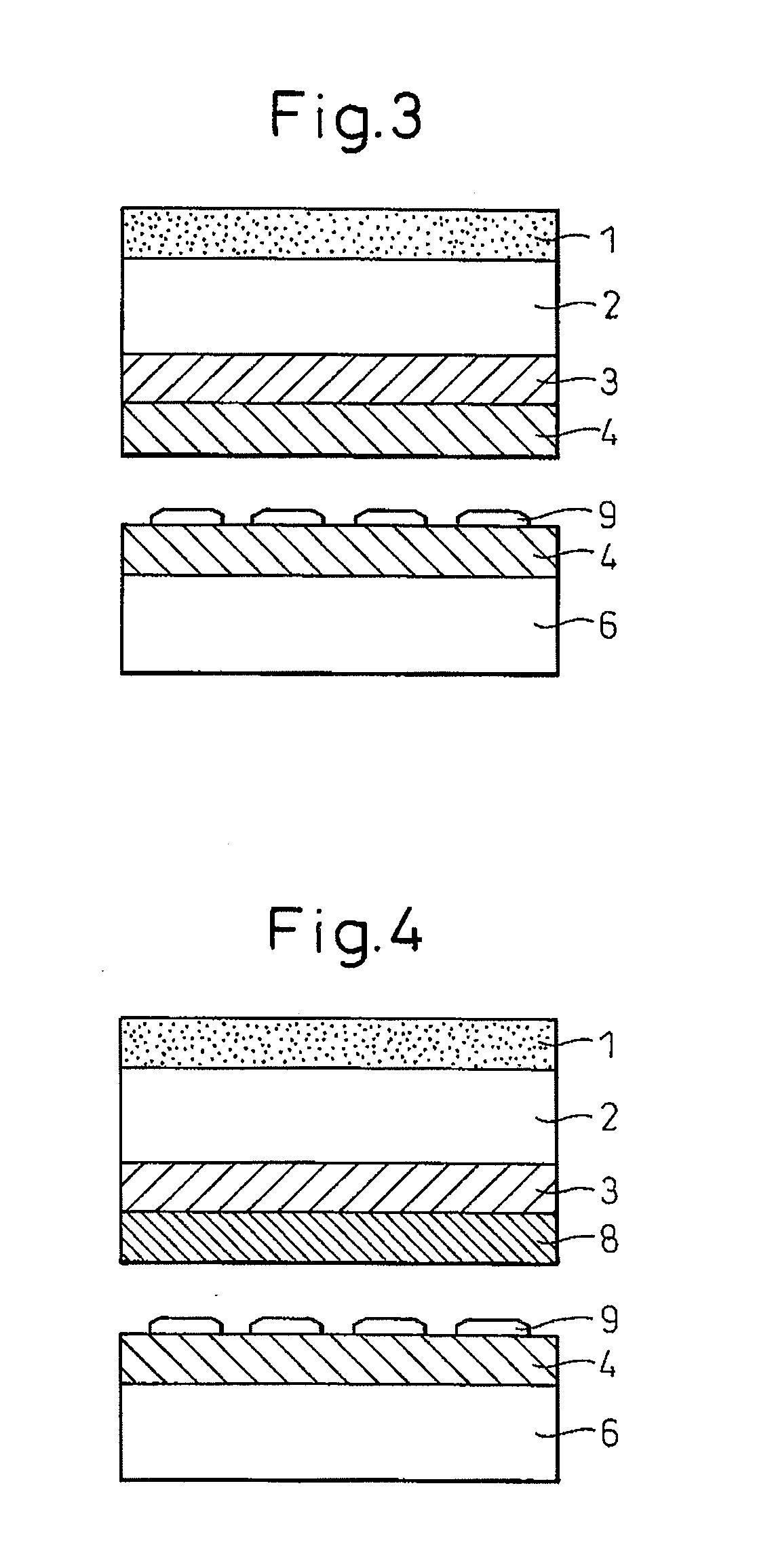
A transparent conductive laminate for obtaining a transparent touch panel improved in the durability in writing which has been required of conventional transparent touch panels and in durability in writing in marginal regions of the transparent touch panel (margin pushing durability). Also provided is a transparent touch panel employing the laminate. The transparent conductive laminate comprises a polymer film and, superposed on at least one side thereof in the following order, a cured resin layer, a transparent conductive layer (1), and another transparent conductive layer (2). The transparent conductive layer (1) is a crystalline transparent conductive layer containing no organic ingredient. The transparent conductive layer (2) comprises: an ionizing-radiation-cured resin, thermoplastic resin, polymer of a metal alkoxide other than alkoxysilanes, or thermally cured / crosslinked resin; and at least one kind of fine particles (A) of a conductive metal oxide or metal which have an average primary-particle diameter of 100 nm or smaller.

Description

TECHNICAL FIELD[0001]The present invention relates to a transparent electroconductive laminate, and a transparent touch panel having the transparent electroconductive laminate.BACKGROUND ART[0002]Mobile information terminals equipped with a display and a transparent touch panel as an input device are becoming more common. A resistive transparent touch panel mostly used as the transparent touch panel is configured such that two transparent electrode substrates, each having a transparent electroconductive layer thereon, are disposed so as to have respective transparent electroconductive layers facing to each other with a gap of about 10 to 100 μm therebetween, and thereby the surfaces of transparent electroconductive layers come into contact with each other only at a portion in which external force is applied. This configuration enables the two transparent electrode substrates to work as a switch. In such a touch panel, for example, a menu can be selected and graphics and letters can ...

Claims


Application Information

Patent Timeline
IPC IPC(8): B32B7/02B32B5/16
CPCG06F3/045Y10T428/258Y10T428/24942Y10T428/25Y10T428/256Y10T428/254B32B27/18B32B33/00H01B5/14G06F3/0412G06F2203/04103B32B2457/208
Inventor ITO, HARUHIKO
Owner TEIJIN LTD
Learn More