Thermoelectric device, manufacturing method for manufacturing thermoelectric device, control system for controlling thermoelectric device, and electronic appliance

a technology for thermoelectric devices and manufacturing methods, applied in the direction of thermoelectric devices, thermoelectric device details, thermoelectric device manufacturing/treatment, etc., can solve the problems of poor productivity and higher cost, reduce the size of the thermoelectric device, and the thermoelectric device to have a higher heat density, etc., to achieve small and sturdy structure, high heat density, and high efficiency

Inactive Publication Date: 2010-10-21
SONY CORP
View PDF6 Cites 7 Cited by
  • Summary
  • Abstract
  • Description
  • Claims
  • Application Information

AI Technical Summary

Benefits of technology

[0032]According to this embodiment of the present invention, the p-type thermoelectric elements are electrically connected to the n-type thermoelectric elements at junction areas of the p-type and n-type thermoelectric elements. The p-type and n-type thermoelectric elements are connected to each other without arranging electrodes therebetween, and thus the contact electrical resistance between the p-type thermoelectric elements and the n-type thermoelectric elements is reduced and a higher heat density is achieved. Since the first insulators are arranged between the p-type thermoelectric elements and the n-type thermoelectric elements, spaces between the p-type thermoelectric elements and the n-type thermoelectric elements are not necessary to spatially insulate the p-type thermoelectric elements from the n-type thermoelectric elements. Thus, a small and sturdy structure is achieved. Since this thermoelectric device is made compact, the thermoelectric device can be locally arranged at the heat source. Moreover, since the thermoelectric device has a higher heat density, heat released from this heat source is efficiently absorbed.
[0033]According to the thermoelectric device according to the embodiments of the present invention, a thermoelectric device is realized whose contact electrical resistance between thermoelectric elements is reduced and that has a higher heat density and a small and sturdy structure. Moreover, according to the embodiments of the present invention, a control system for controlling the thermoelectric device and an electric appliance including the thermoelectric device are provided.
[0034]According to the manufacturing method for manufacturing the thermoelectric device, manufacturing cost is kept low, mass production is made possible, and the size of the thermoelectric device is allowed to be selected with greater flexibility.

Problems solved by technology

Moreover, the p-type thermoelectric elements and the n-type thermoelectric elements are arranged so as to be spaced apart from each other, and thus it is difficult to cause the thermoelectric device to have a higher heat density and reduce the size of the thermoelectric device.
When this manufacturing method is employed, it is necessary to pick up and place the p-type and n-type thermoelectric elements with high accuracy, resulting in poor productivity and higher cost.
However, it is difficult to obtain a temperature difference (ΔT>20° C.
On the other hand, formation of a film whose thickness is sufficient for achieving a sufficient thermoelectric conversion efficiency takes an extremely long time, resulting in higher manufacturing cost.

Method used


Image

  • Thermoelectric device, manufacturing method for manufacturing thermoelectric device, control system for controlling thermoelectric device, and electronic appliance
  • Thermoelectric device, manufacturing method for manufacturing thermoelectric device, control system for controlling thermoelectric device, and electronic appliance
  • Thermoelectric device, manufacturing method for manufacturing thermoelectric device, control system for controlling thermoelectric device, and electronic appliance

Examples


Embodiment Construction

[0054]The following will describe embodiments of the present invention with reference to the drawings.

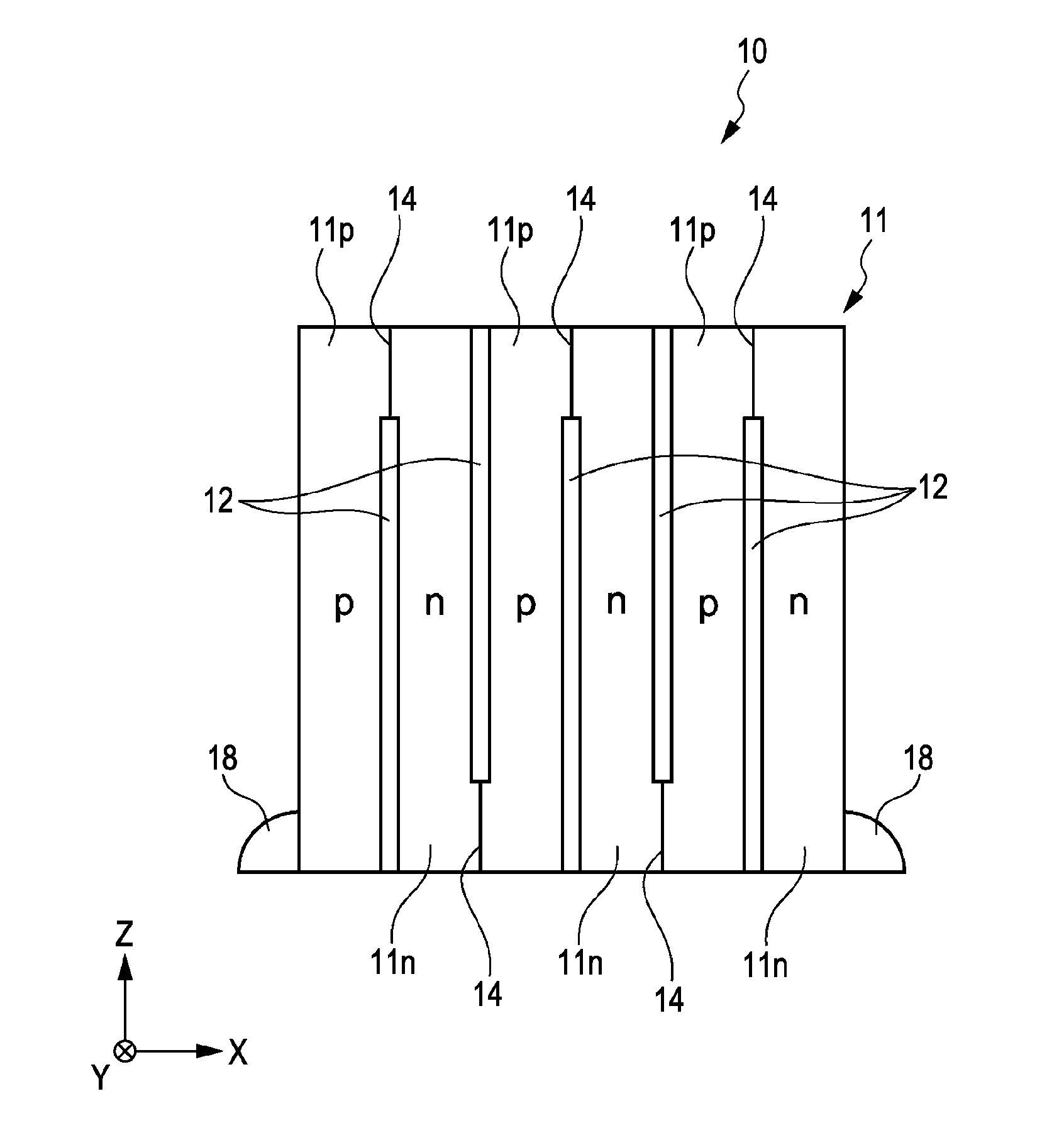
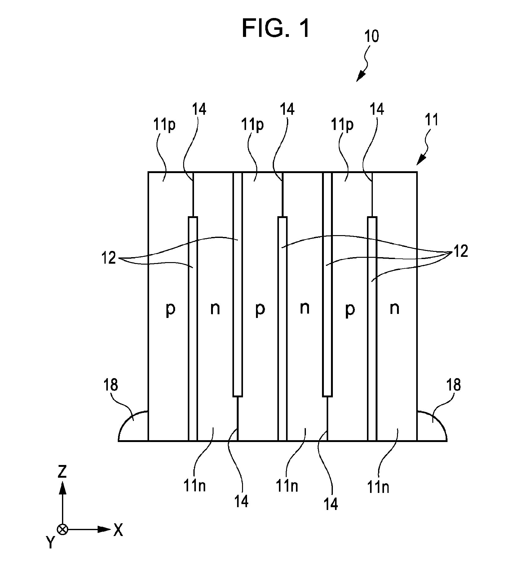
[0055]FIG. 1 is a side view of a thermoelectric device 10 according to an embodiment of the present invention.

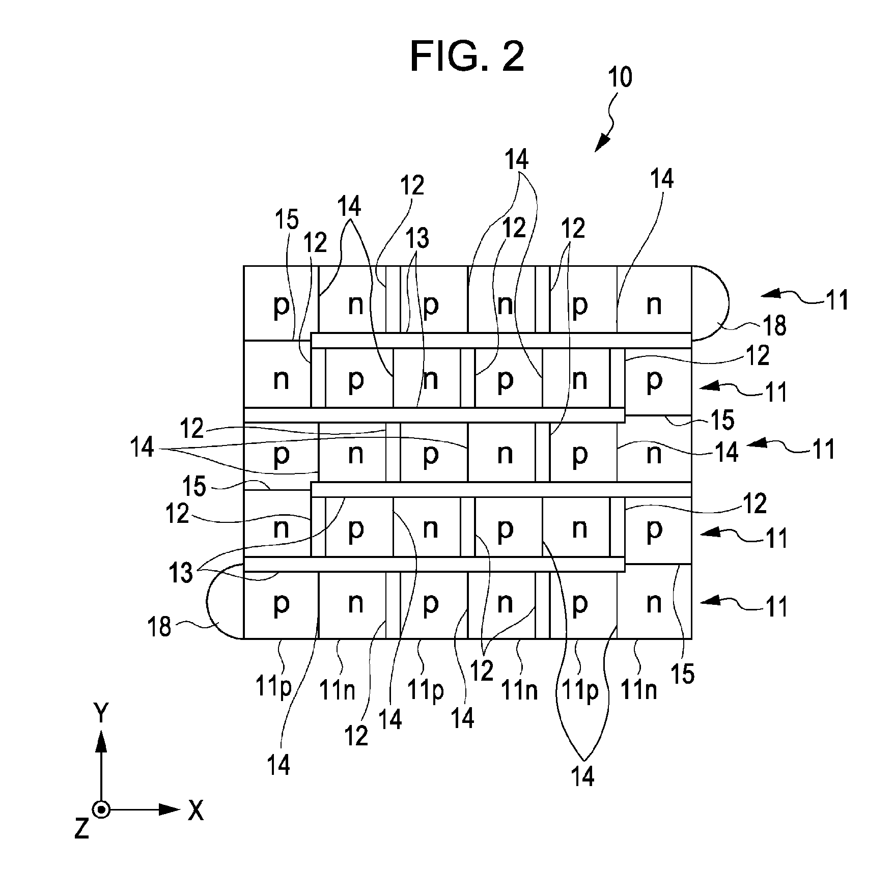
[0056]The thermoelectric device 10 has substantially a rectangular parallelepiped shape or a cube shape. The thermoelectric device 10 includes a plurality of p-type thermoelectric elements 11p, a plurality of n-type thermoelectric elements 11n, a plurality of first insulators 12, and a plurality of second insulators 13 (shown in FIG. 2 and the like).

[0057]As shown in FIG. 1, the p-type thermoelectric elements 11p and the n-type thermoelectric elements 11n, which are provided in an equal number to the p-type thermoelectric elements 11p, are alternately arranged in the direction of the x-axis. For each of the three axes, the size of the p-type thermoelectric elements 11p and the size of the n-type thermoelectric elements 11n are from about 1 μm to about 500 μm. The p-type ther...


PUM

PropertyMeasurementUnit
sizeaaaaaaaaaa
temperatureaaaaaaaaaa
p-type thermoelectricaaaaaaaaaa

Abstract

A thermoelectric device includes rows of thermoelectric elements, each of which includes p-type thermoelectric elements and n-type thermoelectric elements that are alternately arranged in a first direction, the n-type thermoelectric elements each having a junction area electrically connected to one of the p-type thermoelectric elements that adjoins the n-type thermoelectric element; first insulators; and a second insulator. In the thermoelectric device, the first insulators are each arranged between a corresponding one of the p-type thermoelectric elements and one of the n-type thermoelectric elements that adjoins the p-type thermoelectric element. The rows of the thermoelectric elements are arranged in a second direction perpendicular to the first direction and connected to each other. The second insulator is arranged between the rows of thermoelectric elements in such a manner that the p-type thermoelectric elements and n-type thermoelectric elements of the rows of the thermoelectric elements are electrically connected in series.

Description

BACKGROUND OF THE INVENTION[0001]1. Field of the Invention[0002]The present invention relates to thermoelectric devices having a thermoelectric element, manufacturing methods for manufacturing thermoelectric devices, control systems for controlling thermoelectric devices, and electronic appliances.[0003]2. Description of the Related Art[0004]A thermoelectric device in which a thermoelectric element used as a Peltier cooling device is used includes a pair of insulating boards, a plurality of p-type thermoelectric elements, a plurality of n-type thermoelectric elements, and electrodes that are used to connect the p-type thermoelectric elements and the n-type thermoelectric elements. The p-type thermoelectric elements and the n-type thermoelectric elements are alternately arranged so as to be spaced apart from each other and disposed between the pair of the insulating boards. More specifically, the p-type and n-type thermoelectric elements are soldered to electrodes formed on opposing ...

Claims


Application Information

Patent Timeline
Patent Type & Authority Applications(United States)
IPC IPC(8): H01L35/28H05K13/00
CPCH01L23/38H01L35/32H01L35/34Y10T29/49002H01L2924/0002H01L2924/00H10N10/01H10N10/17
Inventor YAZAWA, KAZUAKIISHIDA, YUICHI
Owner SONY CORP
Why Eureka
Try Eureka