Ldmos with self aligned vertical ldd backside drain

a backside drain and self-aligning technology, applied in the field of field-effect transistors, can solve the problems of large device size and large die area consumed by deep diffusion, and achieve the effect of reducing cell pitch and on-resistance rds(on), simple and cost-effectiv

Active Publication Date: 2010-10-21
SEMICON COMPONENTS IND LLC
View PDF4 Cites 4 Cited by
  • Summary
  • Abstract
  • Description
  • Claims
  • Application Information

AI Technical Summary

Benefits of technology

[0004]In accordance with embodiments of the present invention, various techniques are described for reducing cell pitch and on-resistance RDS(on). in LDMOS transistors. Embodiments of the present invention also provide simple and cost-effective method for making LDMOS transistors.

Problems solved by technology

This arrangement tends to result in a large device size.
Such deep diffusion tends to consume additional die area due to side diffusion and misalignment.

Method used


Image

  • Ldmos with self aligned vertical ldd backside drain
  • Ldmos with self aligned vertical ldd backside drain
  • Ldmos with self aligned vertical ldd backside drain

Examples


Embodiment Construction

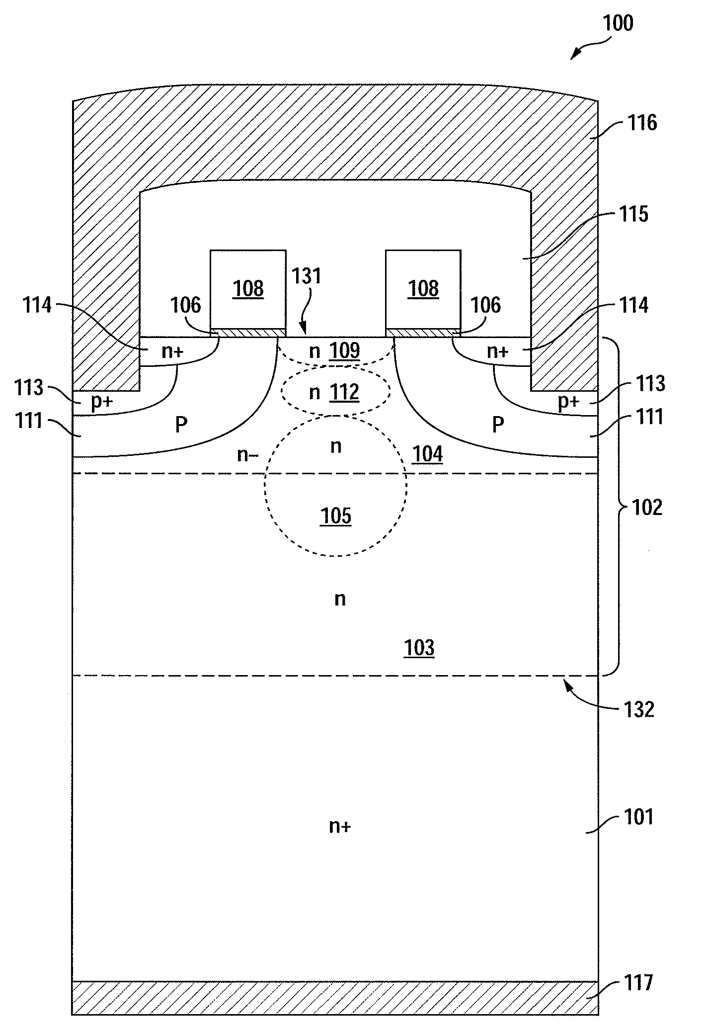
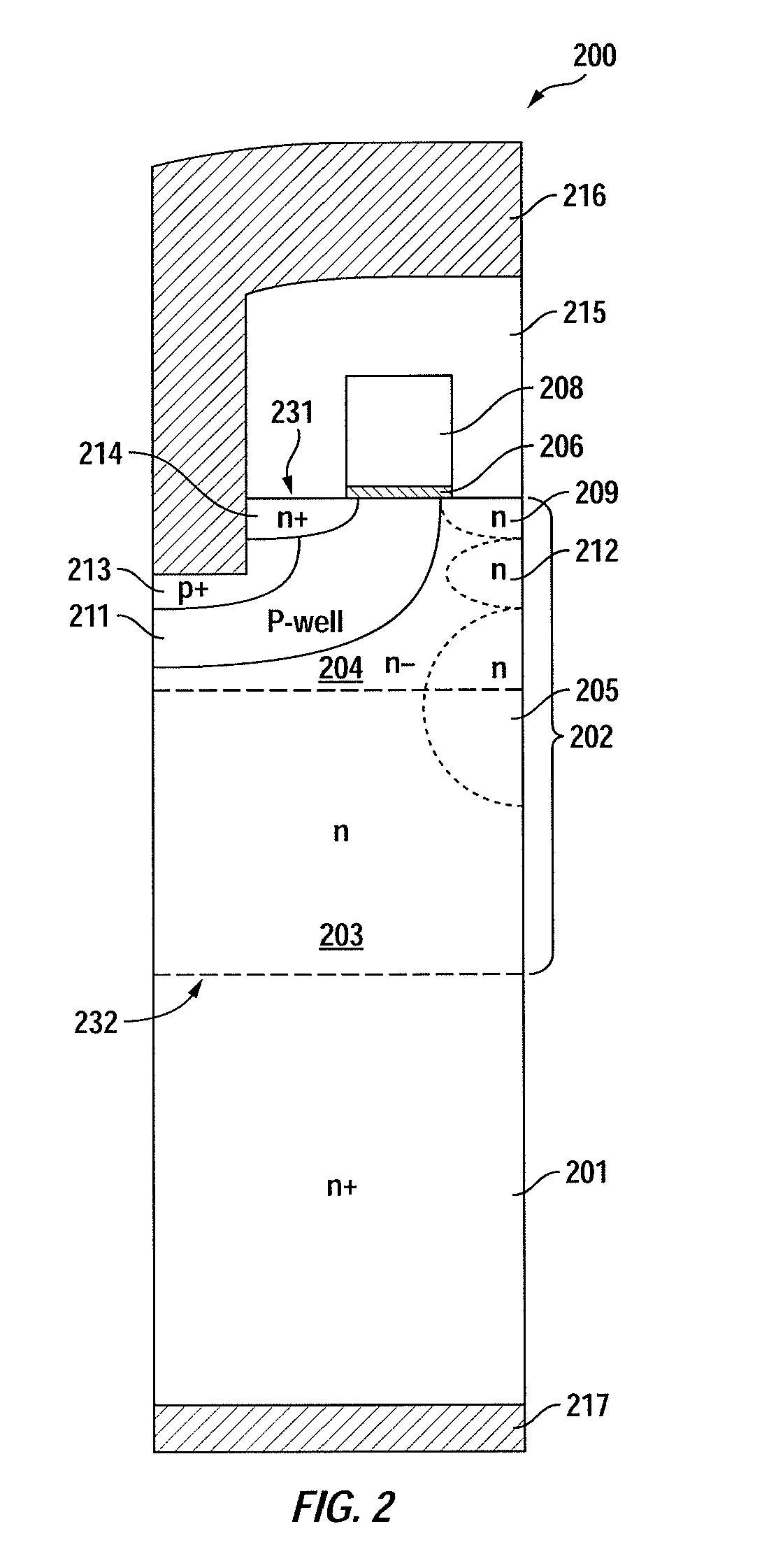
[0030]Embodiments of the present invention relate to LDMOS transistors having a small cell pitch and low resistance RDS(on). In some embodiments of the present invention, one or more LDD regions are arranged together with the sinker region in a vertical stack, with the LDD region(s) being self-aligned to the gate electrodes. This arrangement substantially reduces the cell pitch: (1) by stacking the LDD region(s) and the sinker region that are typically arranged laterally in conventional LDMOS transistors, and (2) by forming the LDD region in a self-aligned manner thus eliminating the provisions for misalignment that need to be made in conventional LDMOS designs.

[0031]In some embodiments, the LDD region(s) and the sinker region are formed between two gate electrodes and are shared by two half cells. The LDD region(s) can be self-aligned to both gate electrodes, and by orienting the LDD region(s) to extend vertically rather than laterally, the LDD region(s) can be formed in the minimu...


PUM


Abstract

A field effect transistor includes a semiconductor region of a first conductivity type having an upper surface and a lower surface, the lower surface of the semiconductor region extending over and abutting a substrate. A well regions of a second conductivity type is disposed within the semiconductor region. The field effect transistor also includes source regions of the first conductivity type disposed in the well regions and a gate electrode extending over each well region and overlapping a corresponding one of the source regions. Each gate electrode is insulated from the underlying well region by a gate dielectric. At least one LDD region of the first conductivity type is disposed in the semiconductor region between every two adjacent well regions such that the at least one LDD region is in contact with the two adjacent well regions between which it is disposed. A sinker region is disposed in the semiconductor region directly underneath the at least one LDD region such that the at least one LDD region and the sinker region are positioned along a vertical orientation between the upper and lower surfaces of the semiconductor region.

Description

BACKGROUND OF THE INVENTION[0001]Embodiments of the invention relate to field effect transistors such as MOSFETs (metal oxide semiconductor field effect transistors) and methods for making field effect transistors.[0002]Laterally Diffused MOS (LDMOS) structures are widely used in high voltage transistors. LDMOS transistors can provide wide frequency range, high linearity, good ruggedness performance, and high breakdown voltages. A conventional LDMOS transistor has its contacted source and drain regions near the surface of the semiconductor wafer, and thus, the current flow in the transistor is more or less along the lateral dimension. In an alternative design, LDMOS transistors have drain contacts along the backside of the die. LDMOS transistors with backside drain typically have a structure arranged in a horizontal sequence of source, polysilicon gate, lightly doped drain (LDD), and sinker region. This arrangement tends to result in a large device size. On the drain side of the tra...

Claims


Application Information

Patent Timeline
Patent Type & Authority Applications(United States)
IPC IPC(8): H01L29/78H01L21/336
CPCH01L29/0878H01L29/7802H01L29/66727H01L29/41766
Inventor MARCHANT, BRUCE D.KINZER, DANIEL M.
Owner SEMICON COMPONENTS IND LLC
Why Eureka
Try Eureka