Method of Employing Slew Dependent Pin Capacitances to Capture Interconnect Parasitics During Timing Abstraction of VLSI Circuits

a technology of slew dependent pin capacitance and timing abstraction, applied in the field of design automation, can solve the problems of increasing the size and complexity of vlsi designs, significant errors in the input-output behavior of the system, and significant errors in delay and slew calculations, so as to speed up the process and achieve accurate timing analysis

Active Publication Date: 2010-10-21
SIEMENS PROD LIFECYCLE MANAGEMENT SOFTWARE INC
View PDF17 Cites 17 Cited by
  • Summary
  • Abstract
  • Description
  • Claims
  • Application Information

AI Technical Summary

Benefits of technology

[0023]These and other objects, aspects and advantages of the invention are achieved by a method and a system for representing the parasitics of an interconnect network as a slew dependent pin capacitance, wherein charge matching between predetermined voltage thresholds is employed. During timing abstraction of a macro, parasitics of interconnects connected to the macro primary inputs are represented as slew dependent pin capacitances in the generated abstract model. Interconnect model order reduction can be advantageously used to speed-up the process. The generated abstract is subsequently used in place of each instance of the macro during chip level hierarchical static timing analysis, thereby facilitating accurate timing analysis for logic components driving the abstracts.

Problems solved by technology

By way of example, a first reduced order model can be analyzed very rapidly, but it may introduce significant errors in the input-output behavior of the system.
However, such a lumped load model can introduce significant errors in the delay and slew calculations while performing a static timing analysis.
With modern chip manufacturing technology scaling to sub-65 nanometers, VLSI designs are increasingly getting larger in terms of size and complexity.
Circuit simulation, while highly accurate for transistor level designs, is run-time intensive.
Accordingly, it is not practical to use in a timing flow where timing runs are made daily during the design cycle of the chip.
In essence, a static timing analysis of such large circuits configured as a single flattened design is run-time prohibitive.

Method used


Image

  • Method of Employing Slew Dependent Pin Capacitances to Capture Interconnect Parasitics During Timing Abstraction of VLSI Circuits
  • Method of Employing Slew Dependent Pin Capacitances to Capture Interconnect Parasitics During Timing Abstraction of VLSI Circuits
  • Method of Employing Slew Dependent Pin Capacitances to Capture Interconnect Parasitics During Timing Abstraction of VLSI Circuits

Examples


Embodiment Construction

[0033]The present invention and the various features and advantageous details thereof are explained more fully with reference to the non-limiting embodiments that are illustrated in the accompanying drawings and detailed in the following description of an embodiment of the invention.

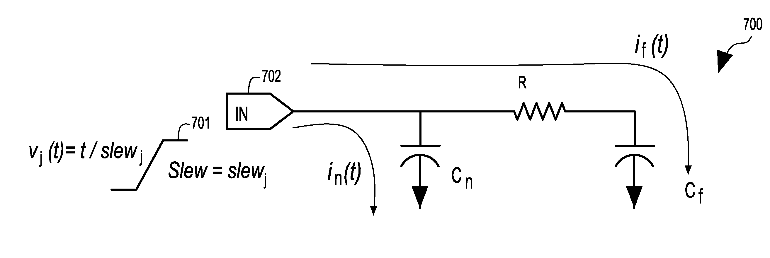
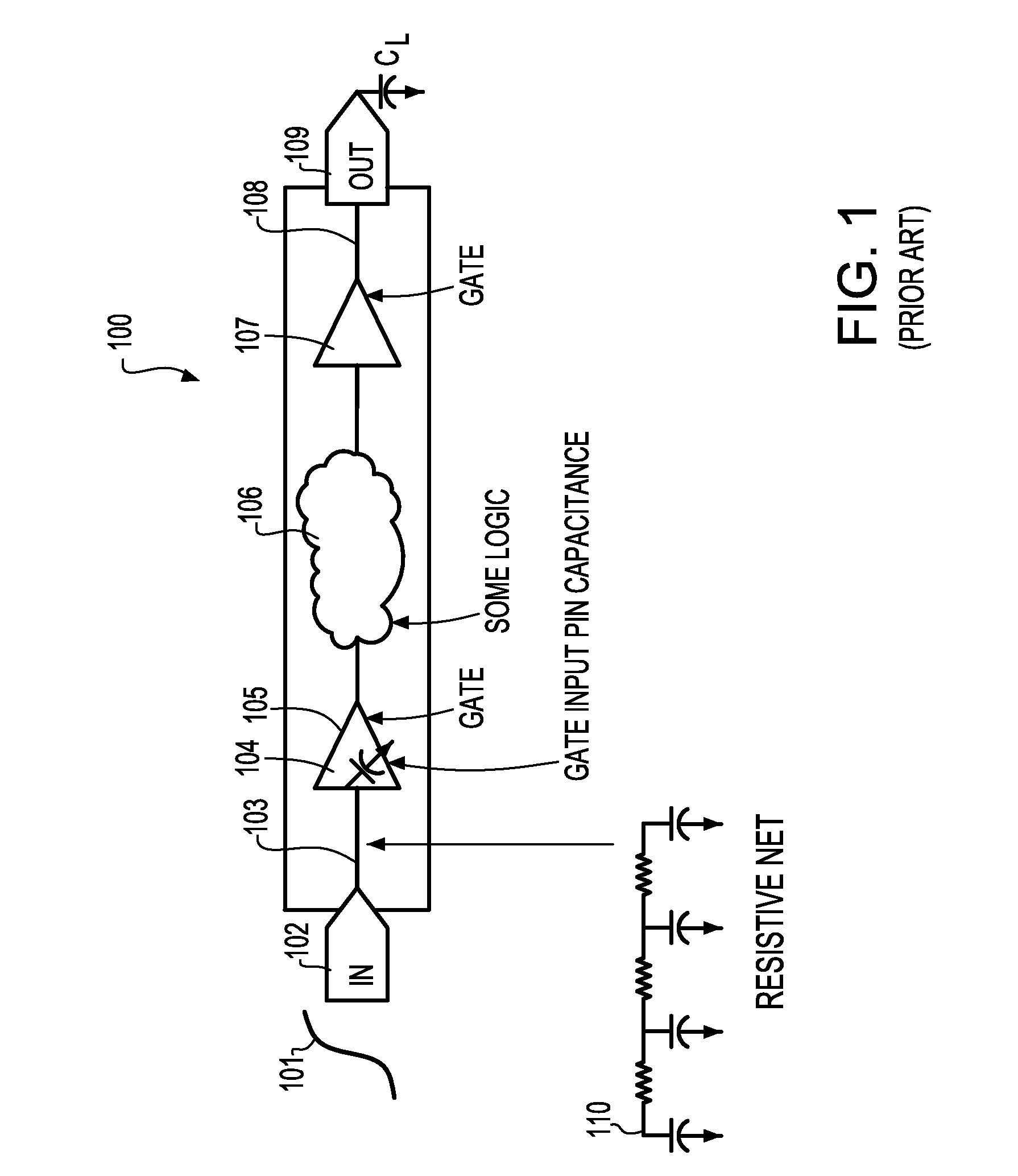
[0034]Typically, abstract models capture the Resistance Capacitance (RC) or Resistance Inductance Capacitance (RLC) parasitics of interconnect networks connected to primary inputs of a macro along with the input pin capacitances of gates fed by the interconnect networks as lumped pin capacitances on the primary inputs. A gate driving such an abstract model during hierarchical chip level STA may incur inaccuracies in delay and slew calculation since it observes a lumped load instead of the real RC or RLC interconnect network. These inaccuracies become significant when the interconnect network connected to the primary input of the abstracted macro is resistive.

[0035]FIG. 4 illustrates the cause of the abov...


PUM


Abstract

A method for converting interconnect parasitics of an interconnect network into slew dependent pin capacitances utilizes charge matching between predetermined voltage thresholds. During timing abstraction of a macro, parasitics of interconnects connected to the primary inputs are represented as slew dependent pin capacitances in an abstract model being created. Interconnect model order reduction is employed to speed the process. The generated abstract is subsequently used in place of each occurrence of the macro during chip level hierarchical static timing analysis, leading to an enhanced accuracy of the timing analysis of the logic components driving the abstracts.

Description

FIELD OF THE INVENTION[0001]The invention generally relates to the field of Design Automation, and more particularly, to the method of modeling interconnect parasitics as slew dependent pin capacitances during timing abstraction of Very Large Scale Integrated (VLSI) circuits.BACKGROUND OF THE INVENTION[0002]Static Timing Analysis (STA) is a key step in the design of high speed Very Large Scale Integrated (VLSI) circuits. It is used to verify that a given VLSI circuit design performs correctly at a required frequency before it is released to manufacturing. STA is performed on a timing graph representation of the design; the points in the design where timing information is desired constitute the nodes or timing points of the graph, while electrical or logic connections between nodes are represented by timing arcs of the graph. STA typically consists of certain fundamental steps that include:[0003]i) delay calculations, which involves modeling and calculating delays across the gates an...

Claims


Application Information

Patent Timeline
Patent Type & Authority Applications(United States)
IPC IPC(8): G06F17/50
CPCG06F17/5031G06F2217/84G06F17/5036G06F30/3312G06F30/367G06F2119/12
Inventor SINHA, DEBJITABBASPOUR, SOROUSHBHANJI, ADILRITZINGER, JEFFREY M.
Owner SIEMENS PROD LIFECYCLE MANAGEMENT SOFTWARE INC
Why Eureka
Try Eureka