Semiconductor device including a mos transistor and production method therefor

a technology of mos transistor and semiconductor device, which is applied in the direction of semiconductor device, basic electric element, electrical apparatus, etc., can solve the problems of reducing the size of the device, increasing the probability of short circuit between the gate and the contact, and difficulty in forming an adequate silicide on the top of the pillar, so as to reduce the narrow width effect, improve the transistor characteristics, and reduce the resistance of the interface

Active Publication Date: 2010-10-28
UNISANTIS ELECTRONICS SINGAPORE PTE LTD
View PDF101 Cites 98 Cited by
  • Summary
  • Abstract
  • Description
  • Claims
  • Application Information

AI Technical Summary

Benefits of technology

[0011]In view of the above circumstances, it is an object of the present invention to, in a vertical transistor, reduce the narrow width effect on a silicide layer on top of a pillar-shaped silicon layer while reducing an interface resistance between the silicide and an upper diffusion layer, to improve transistor characteristics. It is another object of the present invention to achieve a structure free of the occurrence of a short-circuiting between a contact and a gate.
[0031]In a vertical transistor, the present invention makes it possible to reduce the narrow width effect on a silicide layer on top of a pillar-shaped silicon layer while reducing an interface resistance between the silicide and an upper diffusion layer, to improve transistor characteristics. The present invention also makes it possible to achieve a structure free of the occurrence of a short-circuiting between a contact and a gate.

Problems solved by technology

However, the SGT structure illustrated in FIG. 48 has the following problems.
Firstly, in terms of a need for forming a silicide layer on each of upper and lower sides of the pillar-shaped silicon layer to reduce a parasitic resistance in an SGT, a reduction in size of a pillar-shaped silicon layer causes difficulty in forming an adequate silicide on top of the pillar-shaped silicon layer due to the so-called “narrow width effect” on the silicide layer.
In the SGT structure illustrated in FIG. 48, the contact to be formed on top of the pillar-shaped silicon layer is excessively overetched during etching for the contacts, so that a short-circuiting between the gate and the contact becomes more likely to occur.

Method used


Image

  • Semiconductor device including a mos transistor and production method therefor
  • Semiconductor device including a mos transistor and production method therefor
  • Semiconductor device including a mos transistor and production method therefor

Examples


first embodiment

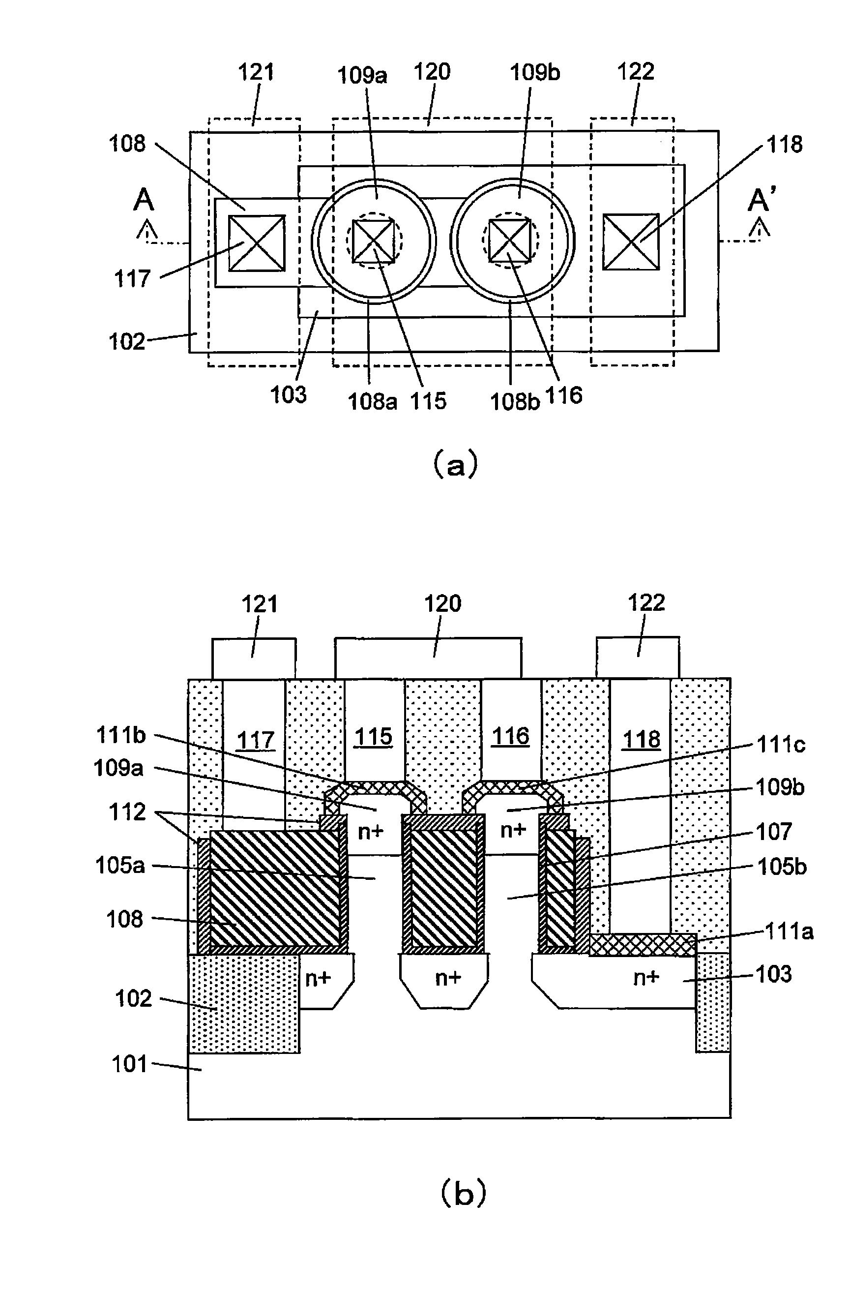
[0080]FIG. 1(a) is a top plan view showing a transistor according to a first embodiment of the present invention, and FIG. 1(b) is a sectional view taken along the line A-A′ in FIG. 1(a). With reference to FIGS. 1(a) and 1(b), a structure of the transistor according to the first embodiment will be described below.

[0081]A silicon substrate 101 is isolated on an element-by-element basis by an element isolation region 102, and two pillar-shaped silicon layers (pillar-shaped semiconductor layers) 105a, 105b are formed on the silicon substrate. A gate dielectric film (first dielectric film) 107 and a gate electrode (108a, 108b) are formed around each of the pillar-shaped silicon layers (pillar-shaped semiconductor layers). In the first embodiment, a High-k film is used as the gate dielectric film (first dielectric film), and a metal film is used as the gate electrode. Alternatively, a silicon oxynitride film formed by oxidation may be used as the gate dielectric film (first dielectric fi...

second embodiment

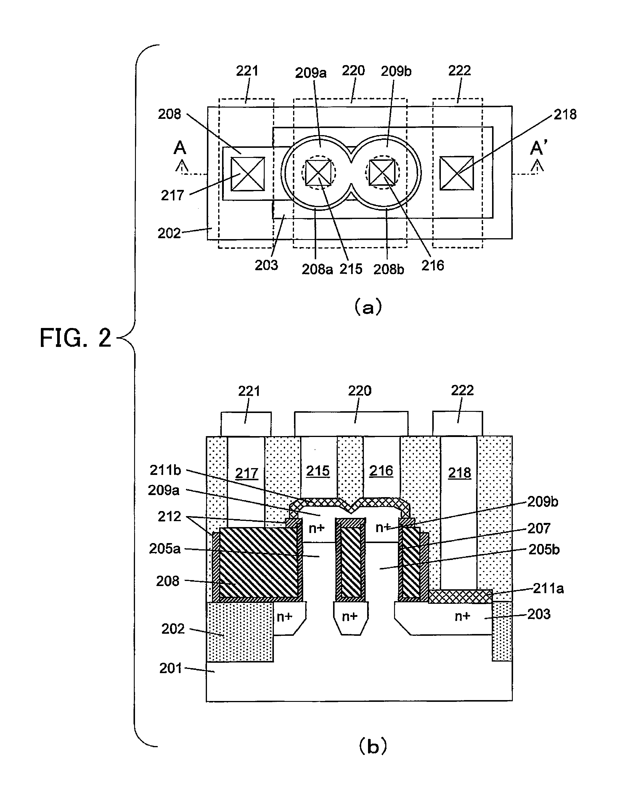
[0103]A second embodiment shows one example where the present invention is applied to a transistor formed by connecting in series two transistors. FIG. 21(a) is a top plan view showing a transistor according to the second embodiment, and FIG. 21(b) is a sectional view taken along the line A-A′ in FIG. 21(a). With reference to FIGS. 21(a) and 21(b), a structure of the transistor according to the second embodiment will be described below. A silicon substrate 601 is isolated on an element-by-element basis by an element isolation 602. Two pillar-shaped silicon layers (pillar-shaped semiconductor layers) 605a, 605b constituting a first transistor, and two pillar-shaped silicon layers (pillar-shaped semiconductor layers) 605c, 605d constituting a second transistor, are formed on the silicon substrate. A gate dielectric film (first dielectric film) 607 and a gate electrode (609a to 609d) are formed around each of the pillar-shaped silicon layers (pillar-shaped semiconductor layers). In the...

third embodiment

[0108]A third embodiment shows one example where the present invention is applied to a CMOS inverter. FIG. 23(a) is a top plan view showing a CMOS inverter according to the third embodiment, and FIG. 23(b) is a sectional view taken along the line A-A′ in FIG. 23(a). In FIGS. 23(a) and 23(b), an interconnection layer 820a connected to an NMOS transistor is connected to GND, and an interconnection layer 820b connected to a PMOS transistor is connected to Vcc. An input signal Vin is input into a gate interconnection layer 808 from an interconnection layer 822, and two interconnection lines 821a, 821b connected from respective upper sides of the NMOS and PMOS transistors are connected to each other through an interconnection layer to output an output signal Vout therefrom. In this manner, a CMOS inverter is formed.

[0109]With reference to FIGS. 23(a) and 23(b), a structure of the CMOS inverter according to the third embodiment will be described below. A silicon substrate 801 is isolated ...


PUM


Abstract

It is intended to provide a semiconductor device including a MOS transistor, comprising: a semiconductor pillar; a bottom doped region formed in contact with a lower part of the semiconductor pillar; a first gate formed around a sidewall of the semiconductor pillar through a first dielectric film therebetween; and a top doped region formed so as to at least partially overlap a top surface of the semiconductor pillar, wherein the top doped region has a top surface having an area greater than that of the top surface of the semiconductor pillar.

Description

RELATED APPLICATIONS[0001]Pursuant to 35 U.S.C. §119(e), this application claims the benefit of the filing date of Provisional U.S. Patent Application Ser. No. 61 / 217,896 filed on Jun. 4, 2009. This application also claims priority under 35 U.S.C. §119(a) to JP2009-109126 filed on Apr. 28, 2009. The entire contents of these applications are hereby incorporated by reference.BACKGROUND OF THE INVENTION[0002]1. Field of the Invention[0003]The present invention relates to a semiconductor device and a production method therefor, and more particularly to a structure and a production method for an SGT (Surrounding Gate Transistor) which is a vertical MOS transistor comprising a pillar-shaped semiconductor layer having a sidewall serving as a channel region, and a gate electrode formed to surround the channel region.[0004]2. Background Art[0005]With a view to achieving higher integration and higher performance of a semiconductor device, an SGT (Surrounding Gate Transistor) has been proposed...

Claims


Application Information

Patent Timeline
Patent Type & Authority Applications(United States)
IPC IPC(8): H01L29/78H01L21/336
CPCH01L21/823885H01L21/84H01L29/0847H01L29/78642H01L29/4975H01L29/66666H01L29/7827H01L29/41741H01L29/78618
Inventor MASUOKA, FUJIOARAI, SHINTARO
Owner UNISANTIS ELECTRONICS SINGAPORE PTE LTD
Why Eureka
Try Eureka