Universal Inter-Layer Interconnect for Multi-Layer Semiconductor Stacks

a multi-layer, interconnecting technology, applied in the direction of instruments, pulse techniques, computation using denominational number representation, etc., can solve the problems of increasing the cost of manufactured chips, reducing the yield of the manufacturing process, and data between the various functional units of the semiconductor chip can become a bottleneck on overall performance, etc., to facilitate interconnection and communication, simplify the circuit layer design

Active Publication Date: 2010-10-28
GLOBALFOUNDRIES US INC
View PDF10 Cites 23 Cited by
  • Summary
  • Abstract
  • Description
  • Claims
  • Application Information

AI Technical Summary

Benefits of technology

[0006]The invention addresses these and other problems associated with the prior art by providing a circuit arrangement and method that utilize a universal, standardized inter-layer interconnect in a multi-layer semiconductor stack to facilitate interconnection and communication between functional units disposed on a stack of semiconductor dies. Each circuit layer in the multi-layer semiconductor stack is required to an inter-layer interface region that is disposed at substantially the same topographic location such that when the semiconductor dies upon which such circuit layers are disposed are arranged together in a stack, electrical conductors disposed within each semiconductor die are aligned with one another to provide an inter-layer

Problems solved by technology

In addition, as feature sizes decrease, and thus as faster and more complex circuits are integrated onto a given semiconductor chip, architects are finding that in many instances the communication of data between the various functional units on a semiconductor chip can become a bottleneck on overall performance.
Furthermore, in general as the size and amount of circuitry integrated into a chip design increases, the yield o

Method used


Image

  • Universal Inter-Layer Interconnect for Multi-Layer Semiconductor Stacks
  • Universal Inter-Layer Interconnect for Multi-Layer Semiconductor Stacks
  • Universal Inter-Layer Interconnect for Multi-Layer Semiconductor Stacks

Examples


Embodiment Construction

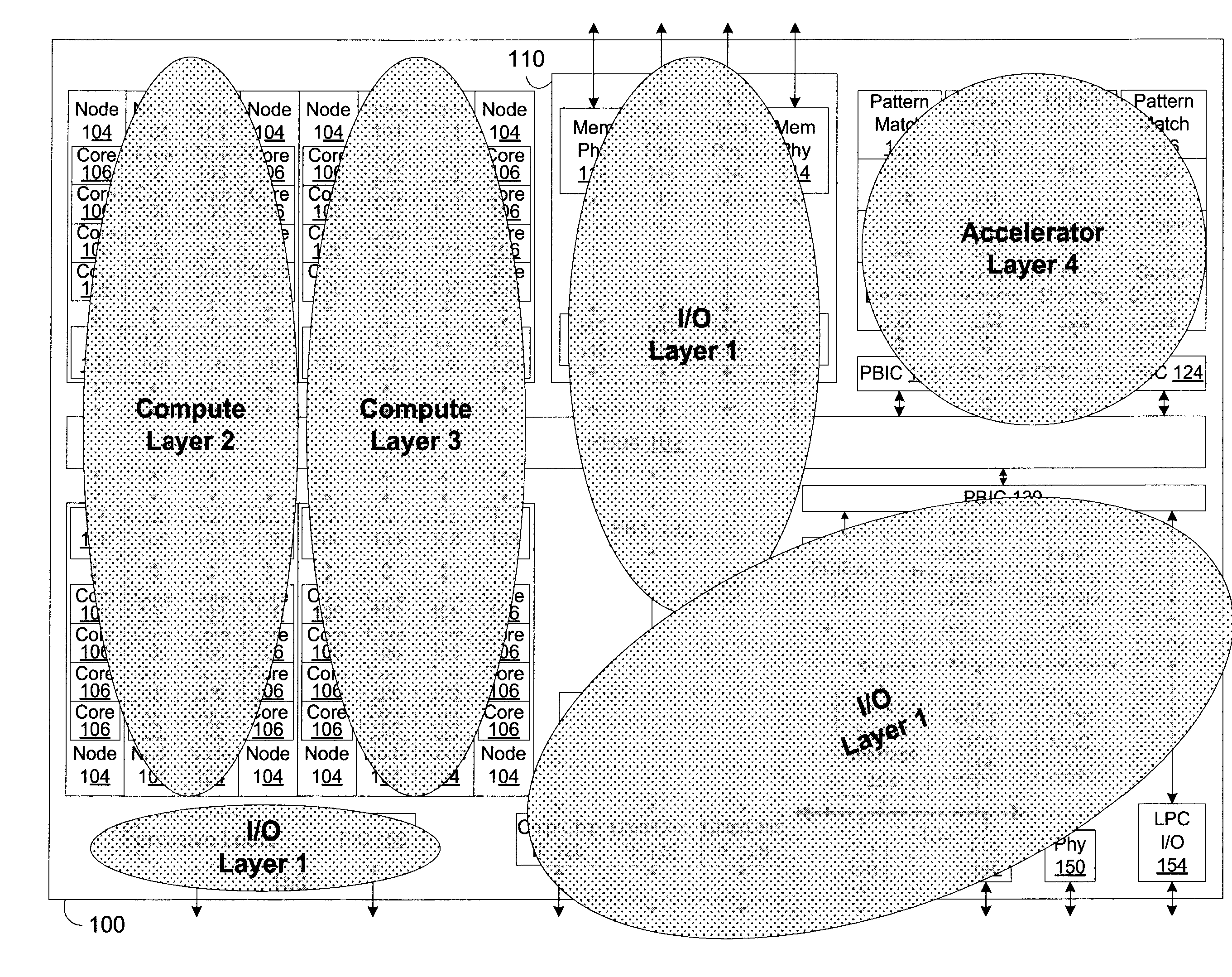
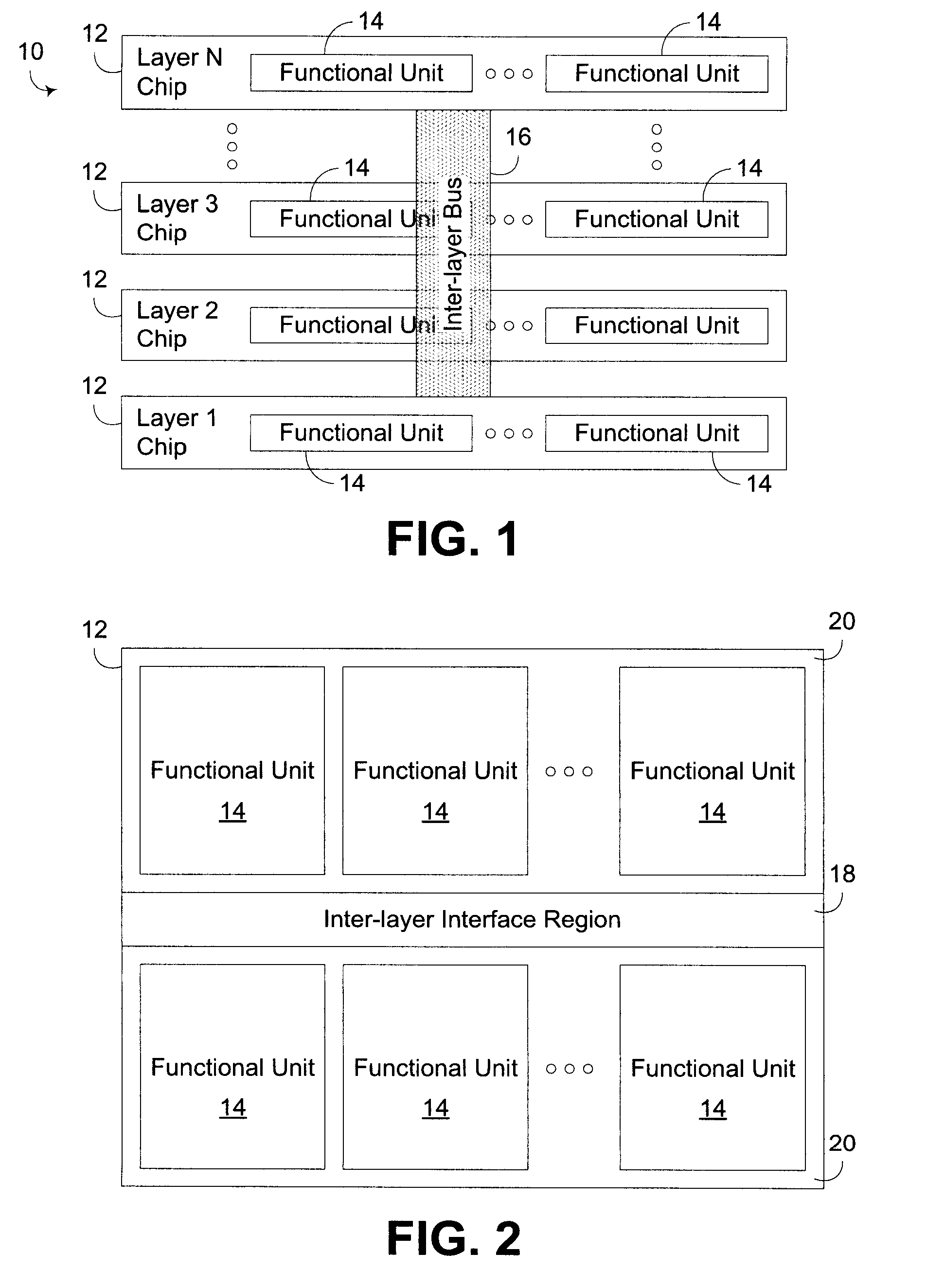
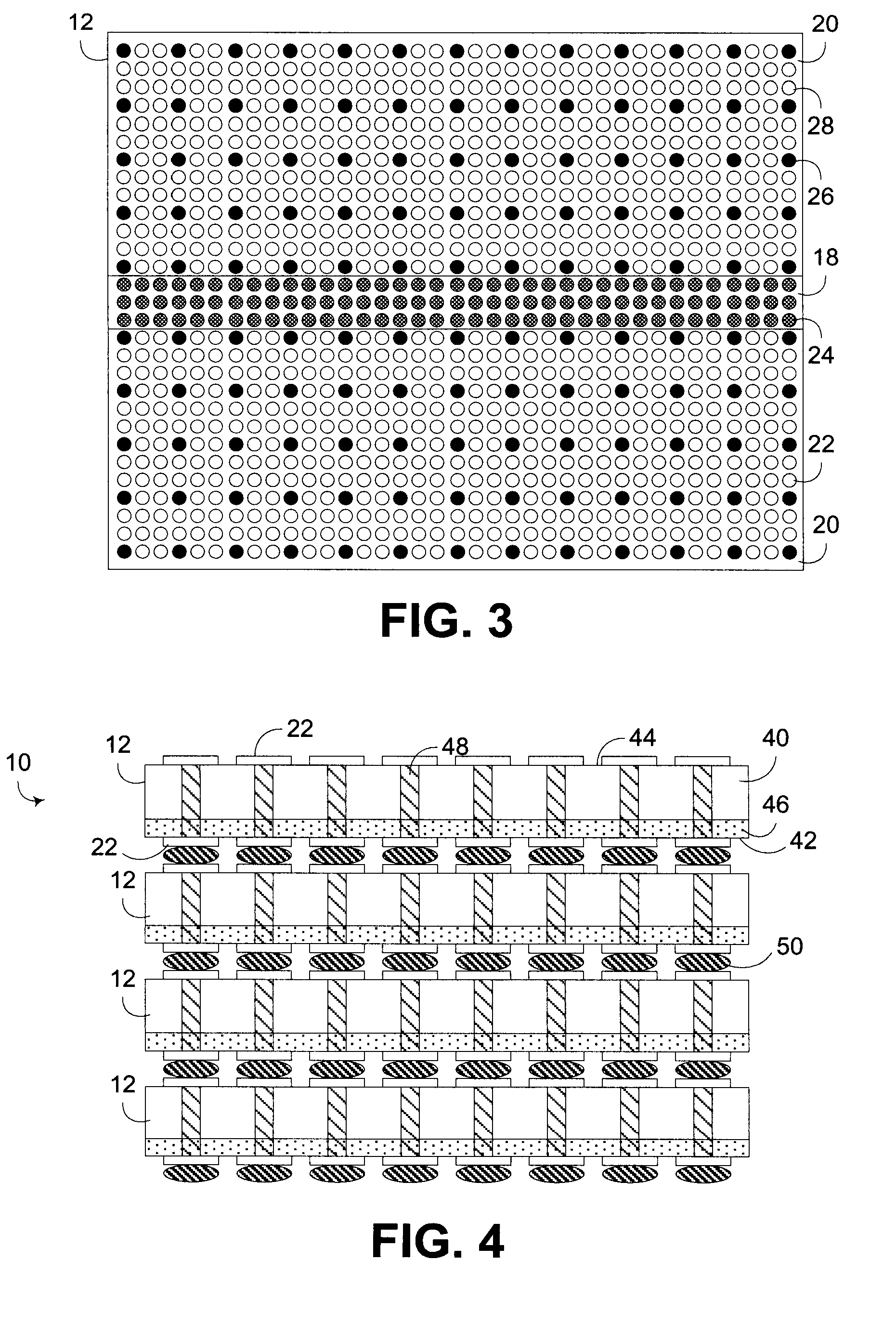
[0026]Embodiments consistent with the invention utilize a universal, standardized inter-layer bus to facilitate communication between functional units disposed in different circuit layers of a multi-layer semiconductor stack. In this regard, an individual circuit layer may be considered to include a two dimensional layout of logic circuitry disposed on a semiconductor substrate. It will be appreciated that, a single circuit layer may include multiple physical layers (e.g., metal layers, dielectric layers, etc.) as a result of fabrication processes, but that these multiple layers collectively define a logic circuit that is essentially laid out across a two dimensional footprint. A multi-layer semiconductor stack therefore includes multiple circuit layers interconnected with one another in an overlapping relationship to effectively define a three dimensional circuit design, adding a vertical or transverse dimension to planar dimensions of the individual circuit layers, and utilizing a...


PUM


Abstract

A circuit arrangement and method utilize a universal, standardized inter-layer interconnect in a multi-layer semiconductor stack to facilitate interconnection and communication between functional units disposed on a stack of semiconductor dies. Each circuit layer in the multi-layer semiconductor stack is required to include an inter-layer interface region that is disposed at substantially the same topographic location such that when the semiconductor dies upon which such circuit layers are disposed are arranged together in a stack, electrical conductors disposed within each semiconductor die are aligned with one another to provide an inter-layer bus that is oriented vertically, or transversely, with respect to the individual circuit layers. Based upon a standardized placement of the inter-layer interface region in each circuit layer, and a standardized arrangement of electrical conductors associated with the inter-layer bus, each circuit layer may designed using a standardized template upon which the design features necessary to implement the inter-layer bus are already provided, thereby simplifying circuit layer design and the interconnection of functional units to the inter-layer bus. In addition, vertically-oriented supernodes may be defined within a semiconductor stack to provide multiple independently-operating nodes having functional units disposed in multiple circuit layers of the stack.

Description

FIELD OF THE INVENTION [0001]The invention is generally related to interconnecting multiple semiconductor dies in a stack and the design of circuit logic therefor.BACKGROUND OF THE INVENTION [0002]As semiconductor technology continues to inch closer to practical limitations in terms of feature size, architects are increasingly focusing on alternative manners of meeting the demands for integrating increasingly complex circuitry onto semiconductor devices, or chips. In addition, as feature sizes decrease, and thus as faster and more complex circuits are integrated onto a given semiconductor chip, architects are finding that in many instances the communication of data between the various functional units on a semiconductor chip can become a bottleneck on overall performance. Communicating data between functional units disposed at opposite ends of a large semiconductor chip (e.g., a 300 or 500 mm2 die size) often requires several clock cycles, as well as significant buffering logic on t...

Claims


Application Information

Patent Timeline
IPC IPC(8): H01L25/00G06F17/50
CPCG06F17/5068H01L25/0657H01L2224/16145H01L2924/01087H01L2225/06541H01L2924/01019H01L2225/06513G06F30/39H01L2224/05001H01L2224/05009H01L2224/05568H01L2924/00014H01L2224/05599H01L2224/05099
Inventor BARTLEY, GERALD K.HOOVER, RUSSELL DEANJOHNSON, CHARLES LUTHERVANDERWIEL, STEVEN PAULVAREKAMP, PATRICK RONALD
Owner GLOBALFOUNDRIES US INC
Why Eureka
Try Eureka