System and method of sensing and removing residual charge from a processed wafer

a technology of residual charge and processing method, which is applied in the direction of electrostatic charge testing/measurement, capacitors, and semiconductor/solid-state device testing/measurement, etc., can solve the problems of substrate not being separated from the wafer, breaking into pieces, or being otherwise damaged

Active Publication Date: 2010-10-28
ADVANCED MICRO FAB EQUIP INC CHINA
View PDF13 Cites 44 Cited by
  • Summary
  • Abstract
  • Description
  • Claims
  • Application Information

AI Technical Summary

Benefits of technology

[0008]What is needed is de-chucking systems and methods of de-chucking that reduce de-chucking failure by discharging residual charges from a processed substrate, and optimize the subsequent de-chucking process by using gathered data from a prior de-chucking run.

Problems solved by technology

However, as residual charges tend to remain on the entire backside of the substrate or at portions of the backside of the substrate, often the substrate fails to separate from the wafer, and / or breaks into pieces or is otherwise damaged during lifting.

Method used


Image

  • System and method of sensing and removing residual charge from a processed wafer
  • System and method of sensing and removing residual charge from a processed wafer
  • System and method of sensing and removing residual charge from a processed wafer

Examples


embodiment 110

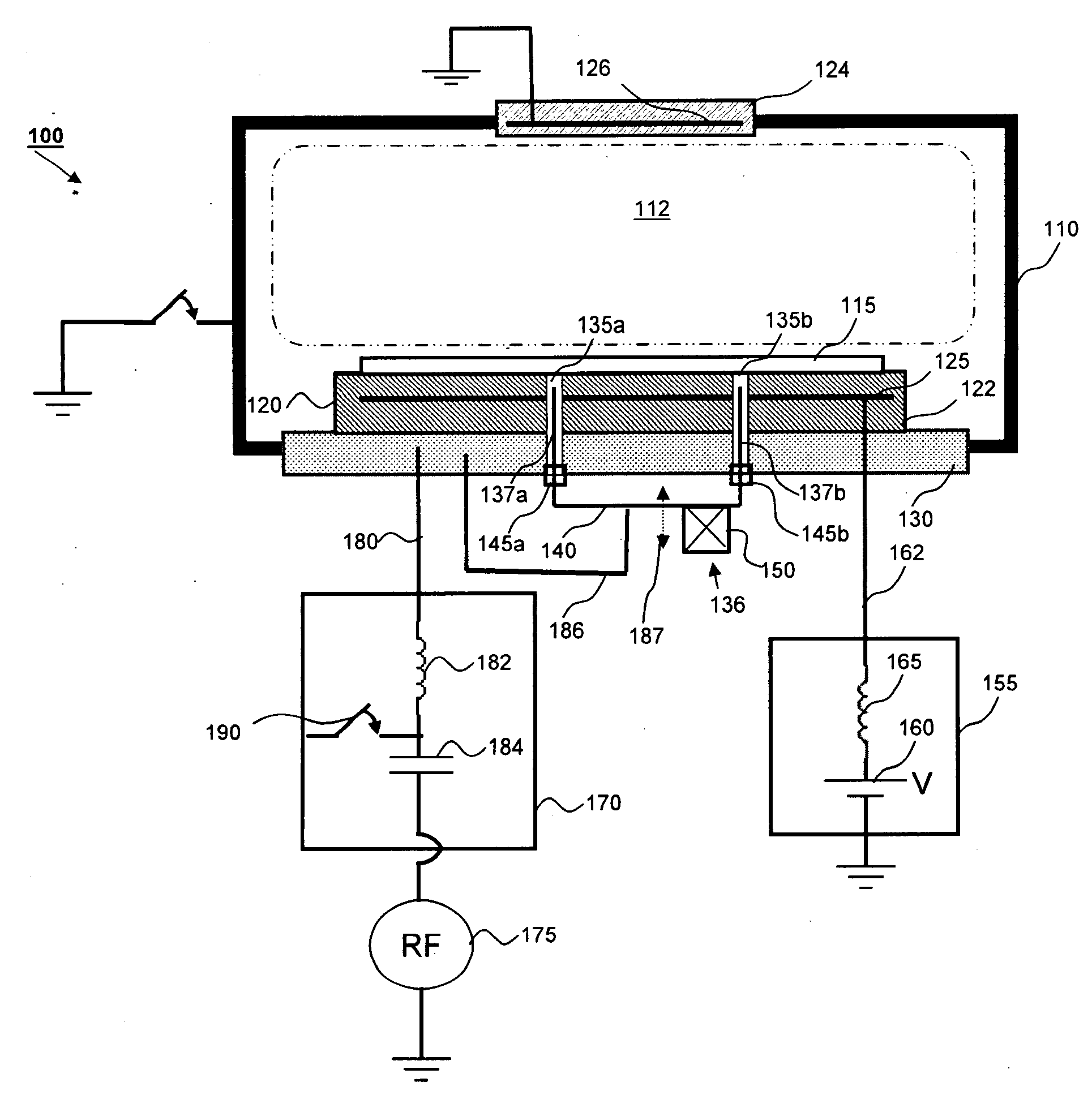
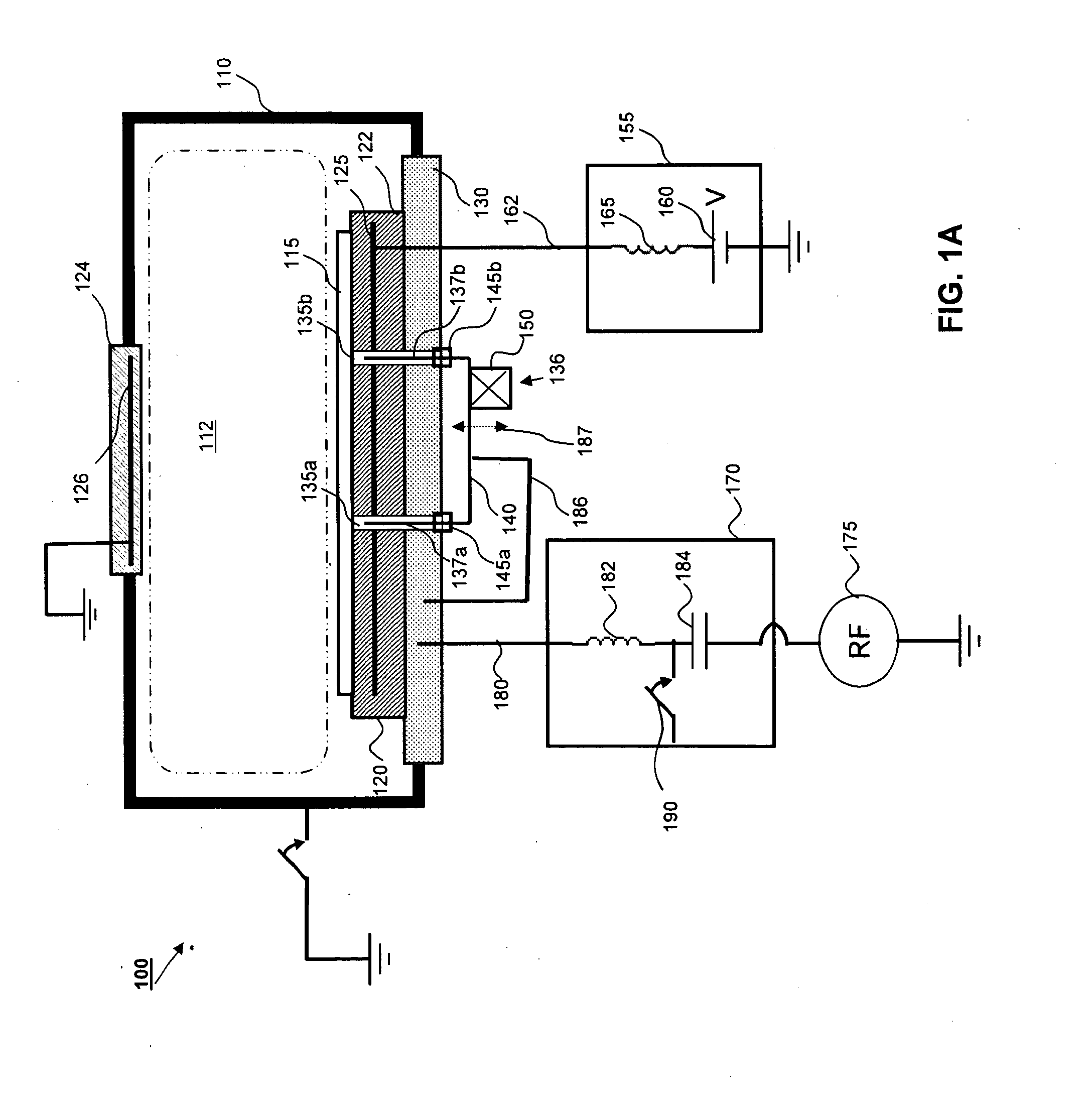
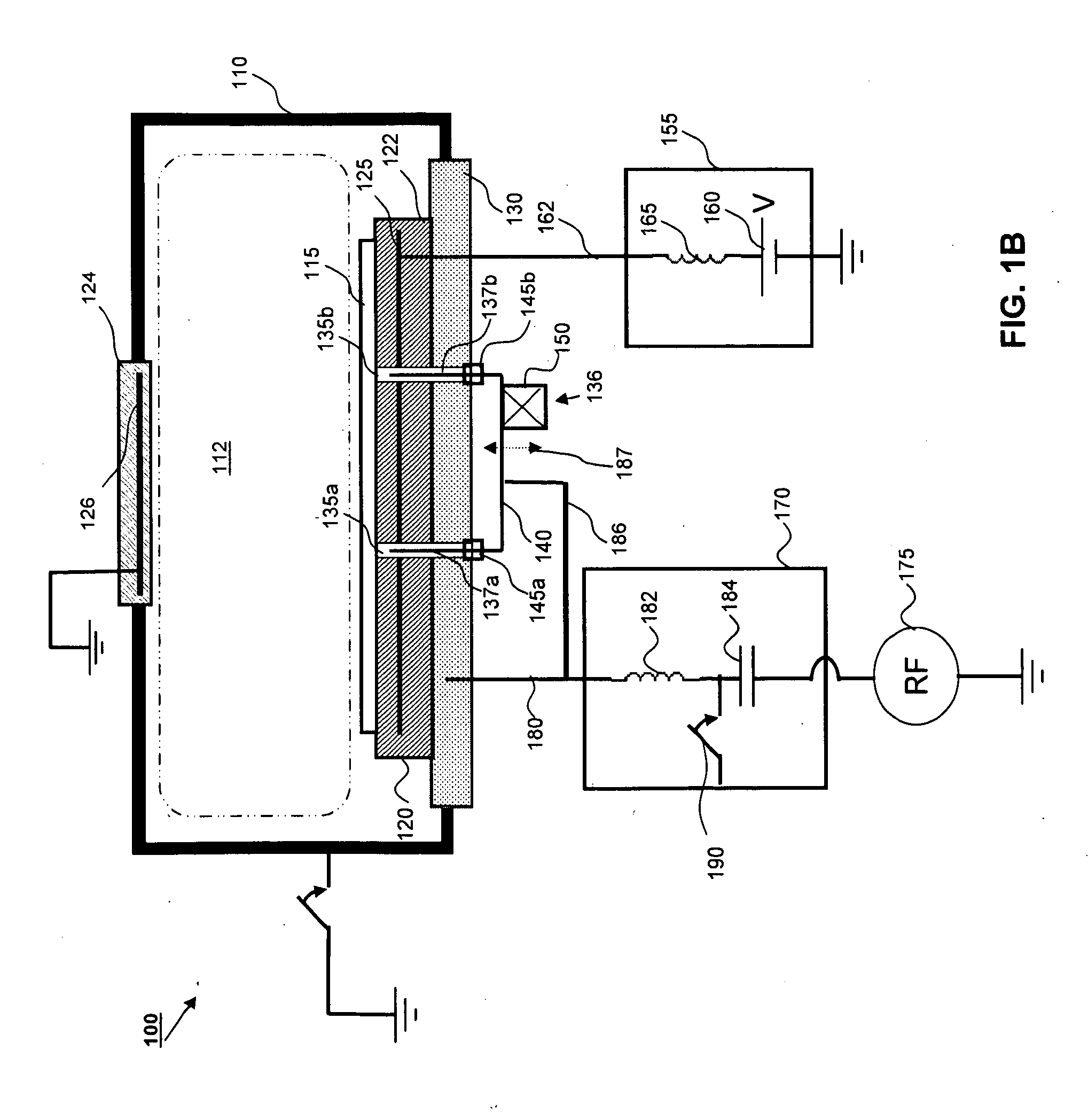
[0032]FIG. 1B illustrates another system embodiment 110, which is identical to processing chamber 100 of FIG. 1A, but depicts an alternative way of connecting ESC pedestal 130 with lift pins 137a-b. In system 110, electrical connector 186 branches out from electrical connector 180. Persons skilled in the art will appreciate that various electrical connection is possible to bring ESC 130 and lift pins 137a-b at the same electrical potential, the invention is not limited by any particular electrical connection.

embodiment 200

[0033]FIG. 2 illustrates another system embodiment 200 of the present invention. System 200 has many elements that are identical to processing chamber 100, as indicated by identical reference numbers. The main difference between processing chamber 100 and system 200 is that switch 190 is not present in system 200. Instead of switch 190, system 200 includes a switch 295 that is configured to establish an alternative discharging path for wafer 115.

[0034]Switch 295, when closed, couples lift pins 137a-b to DC electrode 125 via electrical connector 297. After wafer processing, when RF source 175 is turned off, and switch 295 is closed, as the lift pins touch the bottom surface of wafer 115, DC electrode 125 and wafer 115 attain the same electric potential. In other words, DC electrode 125 and wafer 115 are shorted, and wafer 115 is discharged. Switch 295 may be a vacuum relay or any other type of relay.

[0035]As persons skilled in the art will appreciate, if the goal of the de-chucking p...


PUM


Abstract

Systems and methods for removing residual charge from a processed wafer are described. Removal of residual charge eliminates de-chucking failure that may break or damage the wafer. Residual charge is removed by applying a reverse polarity discharging DC voltage to an electrode embedded in an electrostatic chuck (ESC) supporting the wafer, and providing an outlet to the residual charge to ground via a lift pin assembly. Lift pin assembly is kept at the same potential with respect to a pedestal of the ESC to avoid sparking during the application of RF power to generate plasma. A residual charge sensor is included to sense and measure the amount of residual charge, so that the parameters of the reverse polarity discharging voltage can be adjusted in a subsequent de-chucking operation.

Description

RELATED APPLICATIONS [0001]This application claims priority from Chinese Patent Application Serial No. 200910049960.6, which was filed on Apr. 24, 2009, the entire disclosure of which is incorporated herein by reference.BACKGROUNDFIELD OF THE INVENTION [0002]This invention relates to the art of substrate micro-fabrication and, more particularly, to processed substrate discharge and transfer from an electrostatic chuck.RELATED ARTS [0003]Micro-fabrication of substrates is a well know art employed in, for example, fabrication of semiconductors, flat panel displays, light emitting diodes (LED's), solar cells, etc. Various steps in micro-fabrication may include plasma-assisted processes, (such as, plasma enhanced chemical vapor deposition, reactive ion etching, etc.) performed inside a reaction chamber, into which a process gas is introduced. A radio frequency (RF) source is inductively and / or capacitively coupled to the reaction chamber to energize the process gas to form and maintain ...

Claims


Application Information

Patent Timeline
Patent Type & Authority Applications(United States)
IPC IPC(8): H02N13/00
CPCH01L21/6833H01L22/14H01L21/68742
Inventor NI, TUQIANGCHEN, JINYUANWANG, YEDU, RUOXIONOUYANG, LIANG
Owner ADVANCED MICRO FAB EQUIP INC CHINA
Why Eureka
Try Eureka