Bifacial solar cells with overlaid back grid surface

a solar cell and back grid technology, applied in the field of solar cells, can solve the problems of relatively complex design and technology, and thus high cost, and achieve the effect of reducing manufacturing costs, and simplifying the manufacturing process

Inactive Publication Date: 2010-11-04
SUNNUVELLIR SLHF +1
View PDF12 Cites 44 Cited by
  • Summary
  • Abstract
  • Description
  • Claims
  • Application Information

AI Technical Summary

Benefits of technology

[0007]The present invention provides a simplified manufacturing process and the resultant bifacial solar cell (BSC), the simplified manufacturing process reducing manufacturing costs. In at least one embodiment of the invention, the manufacturing method is comprised of the steps of simultaneously diffusing phosphorous onto the front surface of a silicon substrate to form an n+ layer and a front surface junction and onto the back surface of the silicon substrate to form an n+ layer and a back surface junction, removing the phosphor-silicate glass formed during the diffusion step (e.g., by etching with HF), depositing passivation and AR dielectric layers on the front and back surfaces, applying front and back surface contact grids, and firing the front and back surface contact grids. The front and back surface contact grid firing steps may be performed simultaneously. Alternately, the back surface contact grid applying and firing steps may be performed prior to, or after, the front surface contact grid applying and firing steps. The method may further include the step of firing the back surface contact grid through the back junction, leaving a floating junction. The method may further include the step of removing the back surface junction and isolating the front surface junction, this step performed prior to depositing the back surface dielectric. A back surface metal grid may be applied, for example by screen printing or deposition using a shadow mask, after removing the back surface junction and prior to depositing the dielectric layer on the back surface.

Problems solved by technology

Although there are a variety of BSC designs and techniques for fabricating the same, these designs and techniques tend to be relatively complex, and thus expensive.

Method used


Image

  • Bifacial solar cells with overlaid back grid surface
  • Bifacial solar cells with overlaid back grid surface
  • Bifacial solar cells with overlaid back grid surface

Examples


Embodiment Construction

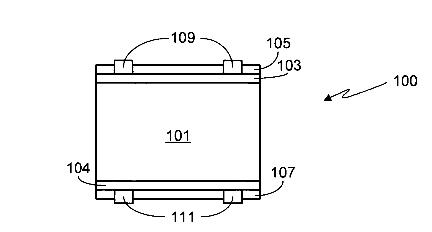
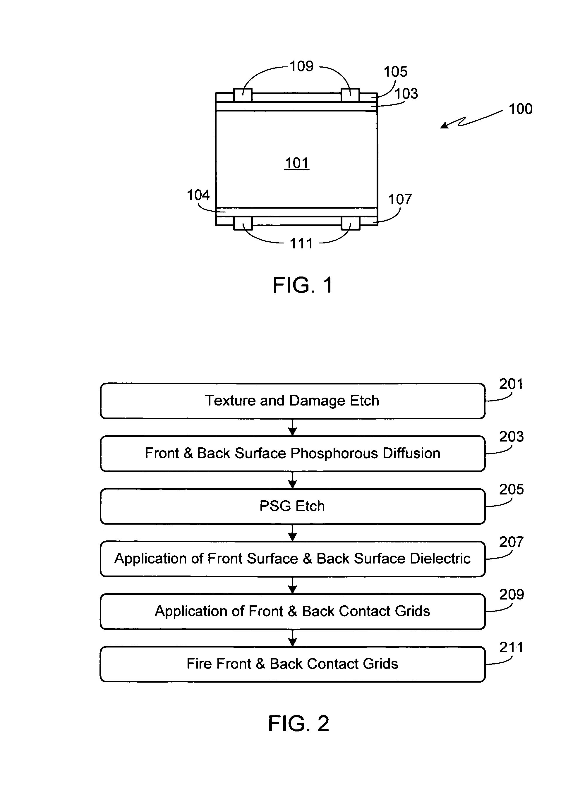
[0019]FIG. 1 illustrates a cross-sectional view of a preferred bifacial solar cell (BSC) structure fabricated in accordance with the procedure described in FIG. 2. Silicon substrate 101 may be of either p- or n-type. In the illustrated device and process of FIGS. 1 and 2, a p-type substrate is used.

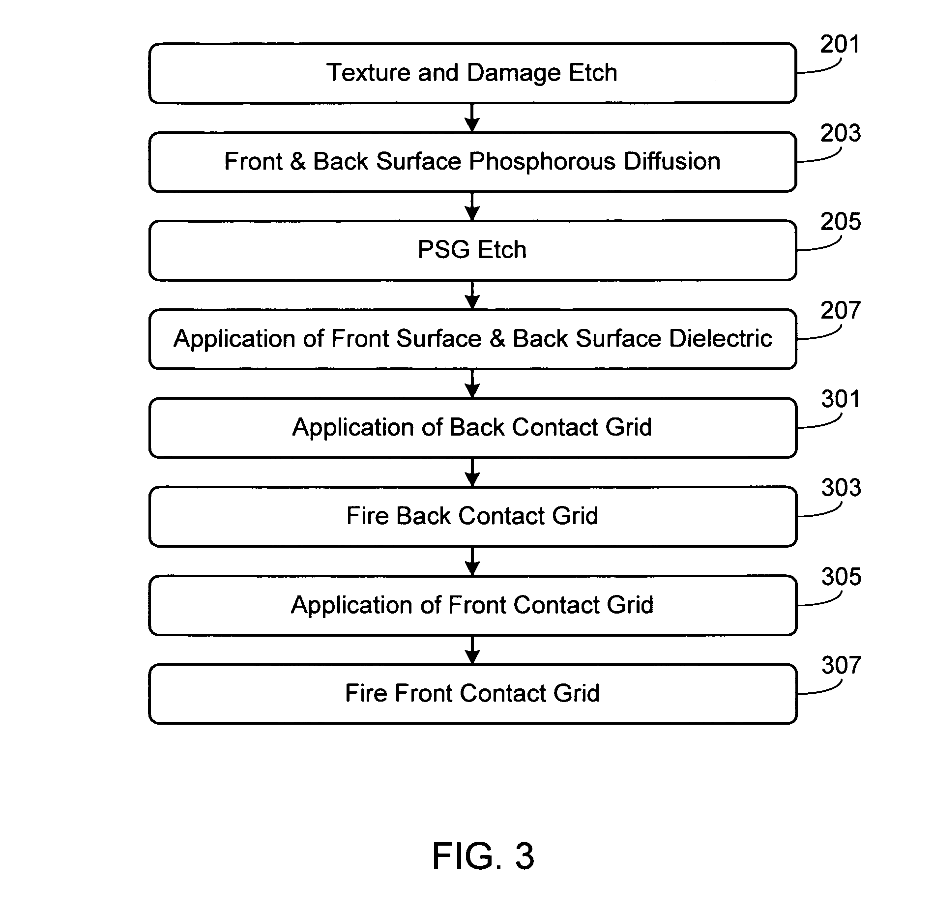
[0020]Initially, substrate 101 is prepared using any of a variety of well-known substrate preparatory processes (step 201). In general, during step 201 saw and handling induced damage is removed via an etching process, for example using a nitric and hydrofluoric (HF) acid mixture. After substrate preparation, phosphorous is diffused onto the front surface of substrate 101, creating n+ layer 103 and a p-n junction at the interface of substrate 101 and n+ layer 103. During this step, phosphorous is also diffused onto the back surface of substrate 101, creating n+ layer 104 and a floating junction. Preferably n+ layer 103 is formed using phosphoryl chloride (POCl3) with a diffusion temperatu...


PUM


Abstract

A simplified manufacturing process and the resultant bifacial solar cell (BSC) are provided, the simplified manufacturing process reducing manufacturing costs. The BSC includes an active region located on the front surface of the substrate, formed for example by a phosphorous diffusion step. After removing the PSG, assuming phosphorous diffusion, and isolating the front junction, dielectric layers are deposited on the front and back surfaces. Contact grids are formed, for example by screen printing. Prior to depositing the back surface dielectric, a metal grid may be applied to the back surface, the back surface contact grid registered to, and alloyed to, the metal grid during contact firing.

Description

CROSS-REFERENCE TO RELATED APPLICATION[0001]This application claims the benefit of the filing date of U.S. Provisional Patent Application Ser. No. 61 / 215,199, filed May 1, 2009, the disclosure of which is incorporated herein by reference for any and all purposes.FIELD OF THE INVENTION[0002]The present invention relates generally to solar cells and, in particular, to an improved structure and manufacturing process for a bifacial solar cell.BACKGROUND OF THE INVENTION[0003]Bifacial solar cells (BSC) may use any of a variety of different designs to achieve higher efficiencies than those typically obtained by a conventional, monofacial solar cell. One such design is shown in U.S. Pat. No. 5,665,175 which discloses a BSC configuration with first and second active regions formed on the front and back surfaces of the BSC, respectively, the two regions separated by a distance λ. The distance λ allows a leakage current to flow between the first and second active regions, thus allowing a sola...

Claims


Application Information

Patent Timeline
Patent Type & Authority Applications(United States)
IPC IPC(8): H01L31/0352H01L31/0232
CPCH01L31/022425H01L31/068H01L31/18H01L31/0684Y02E10/547H01L31/1804Y02P70/50
Inventor KAES, MARTINBORDEN, PETEROUNADJELA, KAMELKRAENZL, ANDREASBLOSSE, ALAINKIRSCHT, FRITZ G.
Owner SUNNUVELLIR SLHF
Why Eureka
Try Eureka