Avalanche capability improvement in power semiconductor devices having dummy cells around edge of active area

a technology of power semiconductor devices and active areas, which is applied in the field of cell structure and device configuration of semiconductor devices, can solve problems such as weakening of the avalanche capability of semiconductor devices, and achieve the effects of enhancing the avalanche capability of the trench mosfet device, enhancing the avalanche capability of the trench igbt device, and enhancing the avalanche capability of the new semiconductor devi

Active Publication Date: 2010-11-04
FORCE MOS TECH CO LTD
View PDF5 Cites 18 Cited by
  • Summary
  • Abstract
  • Description
  • Claims
  • Application Information

AI Technical Summary

Benefits of technology

[0008]One advantage of the present invention is that, dummy cells composed of at least one cell along edge of active area without N+ source (or emitter region for trench IGBT) region are employed according to the present invention, please refer to FIG. 4 and FIG. 5 for top views of closed cell design and stripe cell design of this invention. Said dummy cells having no parasitic bipolar act as buffer cells to absorb avalanche energy at UIS test when gate bias is started to be increased. FIG. 3 shows comparison of UIS current distribution between prior art and the present invention, from which it can be concluded that the value of the UIS current of the present invention is obviously increased while having a distribution much narrower than the prior art.
[0009]Another advantage of the present invention is that, the failed sites after UIS test in this invention become random distribution instead of always occurring near edge of active area, as shown in FIG. 10A, enhancing the avalanche capability of the new semiconductor device.
[0010]Briefly, in a preferred embodiment according to the present invention, as shown in FIG. 6, which also shows the b-b′ section view of a preferred embodiment of FIG. 4. The present invention disclosed a trench MOSFET device formed on a substrate heavily doped with a first semiconductor doping type, e.g., N+ doping type. Onto said substrate, grown an epitaxial layer lightly doped with the same semiconductor doping type as the substrate and a plurality of trenches were etched wherein doped poly was filled within a plurality of trenches to serve as trench gates over a gate oxide layer along the inner surface of said gate trenches. P-body regions are extending between every two gate trenches while N+ source regions formed on its top surface only within active area. Through a thick contact oxide interlayer deposited over epitaxial layer, source-body contact trenches are etched into epitaxial layer for source-body connection. Tungsten plugs acting as the contact metal are filled into the source-body contact trenches to connect said source regions and said body regions to source metal. Dummy cells without N+ source region composed of at least one cell is implemented along edge of active area, helping to enhance avalanche capability of the trench MOSFET device. In termination area, gate metal runner which also serving as metal field plate is formed overlying P body and top surface of epitaxial layer.
[0011]Briefly, in another preferred embodiment according to the present invention, as shown in FIG. 7, which also shows the b-b′ section view of another preferred embodiment of FIG. 4. The trench MOSFET structure disclosed is similar to the structure in FIG. 6 except that there is a deep guard ring under said gate metal runner in termination area.
[0012]Briefly, in another preferred embodiment according to the present invention, as shown in FIG. 8, which also shows the b-b′ section view of another preferred embodiment of FIG. 4. The trench MOSFET structure disclosed is similar to the structure in FIG. 6 except that there are multiple trench floating rings to serve as termination.
[0013]Briefly, in another preferred embodiment according to the present invention, as shown in FIG. 9, the present invention disclosed a trench IGBT device formed on a substrate heavily doped with a second semiconductor doping type, e.g., P+ doping type. Onto said substrate, a heavily doped epitaxial layer and another lightly doped epitaxial layer are subsequently formed with the opposite doping type to the substrate. A plurality of trenches were etched within lightly doped epitaxial layer and filled with doped poly to serve as trench gates over a gate oxide layer along the inner surface of the gate trenches. P-body regions are extending between every two gate trenches with N+ emitter regions top its top surface only within active area. Through a thick contact oxide interlayer deposited over epitaxial layer, emitter-base contact trenches are etched into epitaxial layer for emitter-base connection. Tungsten plugs acting as the contact metal are filled into the emitter-base contact trenches to connect the emitter regions and the body regions to emitter metal. Dummy cells without N+ emitter region composed of at least one cell is implemented along edge of active area, helping to enhance avalanche capability of the trench IGBT device. In termination area, gate metal runner which also serving as metal field plate is formed over deep guard ring and multiple floating rings.

Problems solved by technology

Since the cells are most nearest gate metal pad and gate runner (refer to FIG. 1A), the gate of the cells near the active edge are turned on first when gate bias is increasing for turning on channel, resulting the parasitic bipolar turning on first near the active edge, thus weakening the avalanche capability of semiconductor device.

Method used


Image

  • Avalanche capability improvement in power semiconductor devices having dummy cells around edge of active area
  • Avalanche capability improvement in power semiconductor devices having dummy cells around edge of active area
  • Avalanche capability improvement in power semiconductor devices having dummy cells around edge of active area

Examples


Embodiment Construction

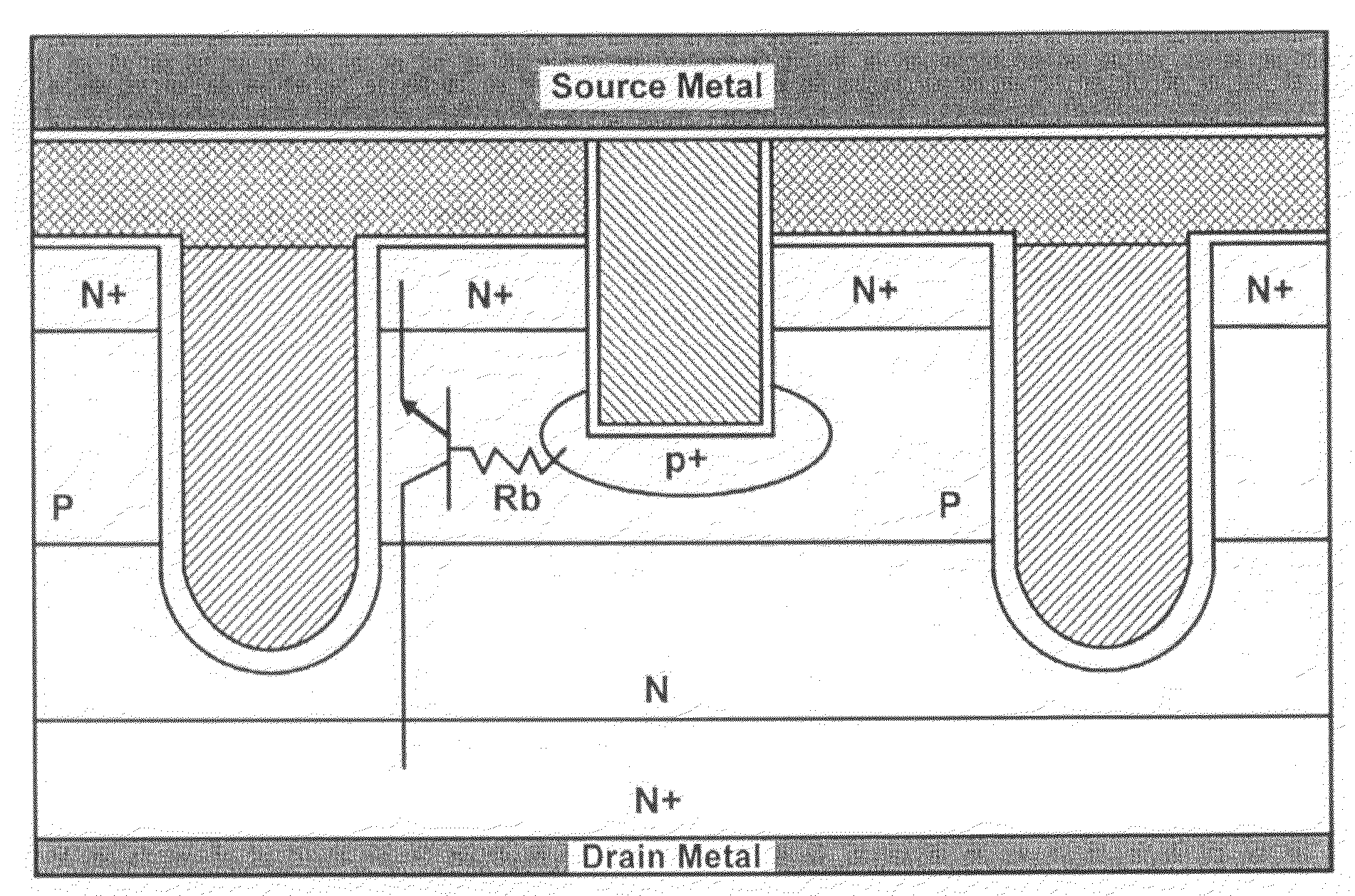
[0031]Please refer to FIG. 6 for a preferred embodiment of this invention showing the b-b′ cross section of FIG. 4 where an N-channel trench MOSFET with dummy cells at the edge of active area formed on a heavily N+ doped substrate 600 coated with back metal 690 on rear side as drain. Onto said substrate 600, a lightly N doped epitaxial layer 601 is grown, and a plurality of trenches is etched wherein. Doped poly is filled into the gate trenches padded with a gate insulation layer 620 formed over the inner surface of gate trenches to form trenched gates 610. P-body regions 602 are extending between every adjacent trench gates 610 with N+ source region 603 near the top surface only within active area 640. Trench source-body contacts filled with tungsten plug 612 are formed penetrating through a thick contact oxide interlayer 604 with contact p+ implantation area 622 around each the source-body contact bottom to contact source region 603 and P-body region 602 to source metal 605. Dummy...


PUM


Abstract

A structure of power semiconductor device having dummy cells around edge of active area is disclosed. The UIS test result of said improved structure shows that failed site after UIS test randomly located in active area which means avalanche capability of the semiconductor power device is enhanced by implementation of the dummy cells.

Description

FIELD OF THE INVENTION [0001]This invention relates generally to the cell structure and device configuration of semiconductor devices. More particularly, this invention relates to an improved device configuration with dummy cells around edge of active area to enhance the avalanche capability of semiconductor devices.BACKGROUND OF THE INVENTION[0002]The unclamped inductive switching test (UIS test) is used to evaluate avalanche capability of a semiconductor power device by measuring UIS current at breakdown voltage. Yet, failed site after UIS test always occur near edge of active area of semiconductor power device of prior art, as shown in FIG. 1A to FIG. 1C.[0003]FIG. 1A shows the top view a trench MOSFET of prior art while FIG. 1B shows its a-a′ cross section view. Refer to FIG. 1B, this device is formed on N+ substrate 100 on which an N doped epitaxial layer 102 is grown. A plurality of trenches are etched inside said epitaxial layer 102 and filled with doped poly within trenches ...

Claims


Application Information

Patent Timeline
Patent Type & Authority Applications(United States)
IPC IPC(8): H01L29/739H01L29/78
CPCH01L27/0255H01L29/7813H01L29/0619H01L29/0696H01L29/0865H01L29/1095H01L29/402H01L29/407H01L29/41766H01L29/42372H01L29/4238H01L29/7397H01L29/7804H01L29/7811H01L29/0615H01L2224/0603
Inventor HSIEH, FU-YUAN
Owner FORCE MOS TECH CO LTD
Why Eureka
Try Eureka