
Integrated Circuit Design using DFM-Enhanced Architecture

Inactive Publication Date: 2010-11-04
TAIWAN SEMICON MFG CO LTD
View PDF12 Cites 25 Cited by
  • Summary
  • Abstract
  • Description
  • Claims
  • Application Information

AI Technical Summary

Benefits of technology

[0007]The advantageous features of the present invention include improved performance of integrated circuits, reduced power consumption in the integrated circuits, and reduced manufacturing cost.

Problems solved by technology

For example, the length of diffusion (LOD) significantly affects the performance of the integrated circuits.
However, existing ASIC design methods do not adequately take the DFM effects into account.
However, at this stage, it is too late to change the circuit to take full advantage of the DFM effects.

Method used


Image

  • Integrated Circuit Design using DFM-Enhanced Architecture
  • Integrated Circuit Design using DFM-Enhanced Architecture
  • Integrated Circuit Design using DFM-Enhanced Architecture

Examples


Embodiment Construction

[0011]The making and using of the embodiments of the present invention are discussed in detail below. It should be appreciated, however, that the embodiments provide many applicable inventive concepts that can be embodied in a wide variety of specific contexts. The specific embodiments discussed are merely illustrative of specific ways to make and use the invention, and do not limit the scope of the invention.

[0012]A novel design-for-manufacturing (DFM) aware standard cell libraries in accordance with an embodiment of the present invention is provided. A method of designing integrated circuits using the DFM-aware standard cell library is also provided. The variations of the embodiment are discussed. Throughout the various views and illustrative embodiments of the present invention, like reference numbers are used to designate like elements.

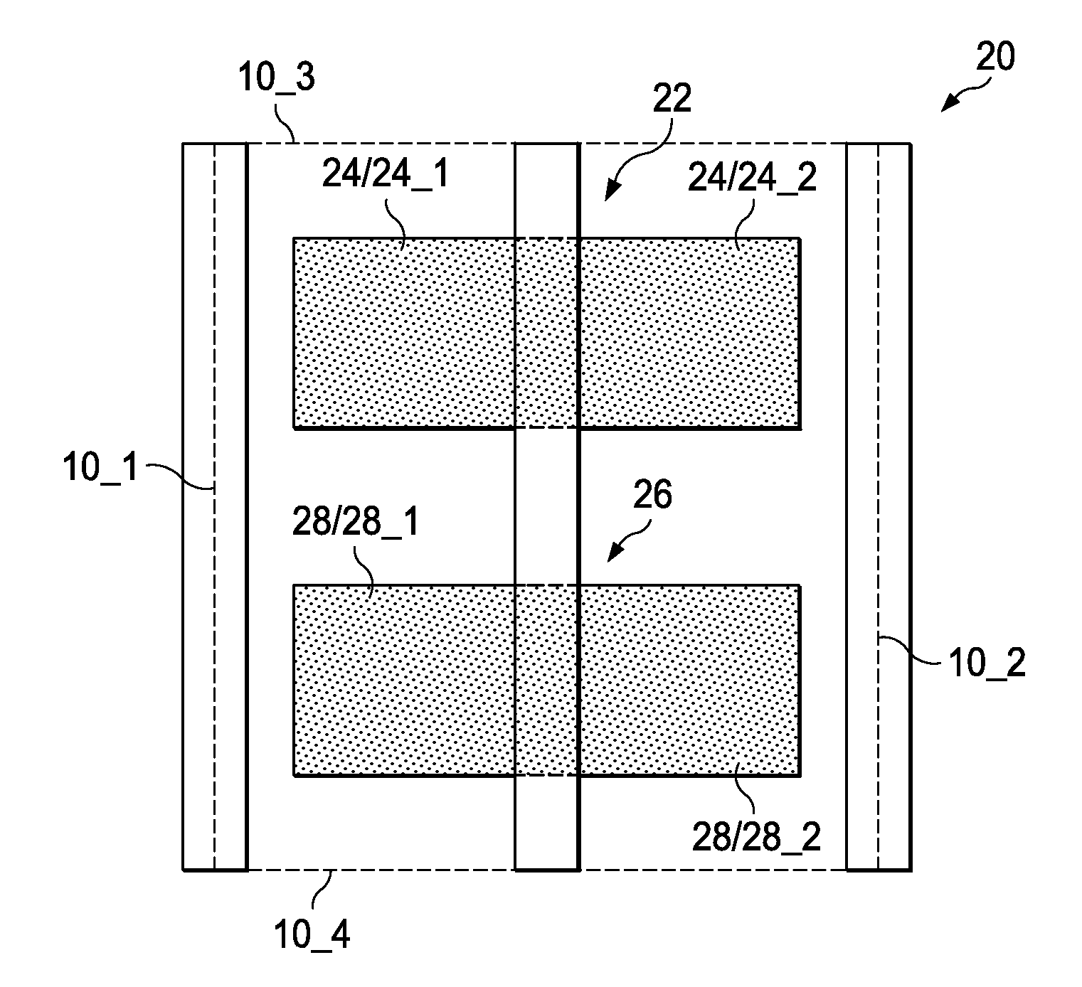
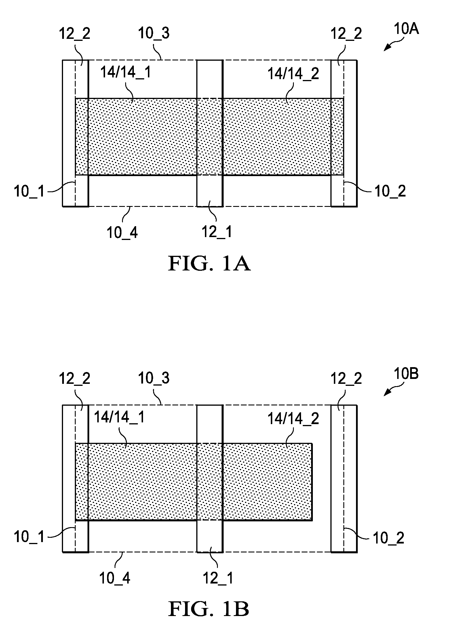
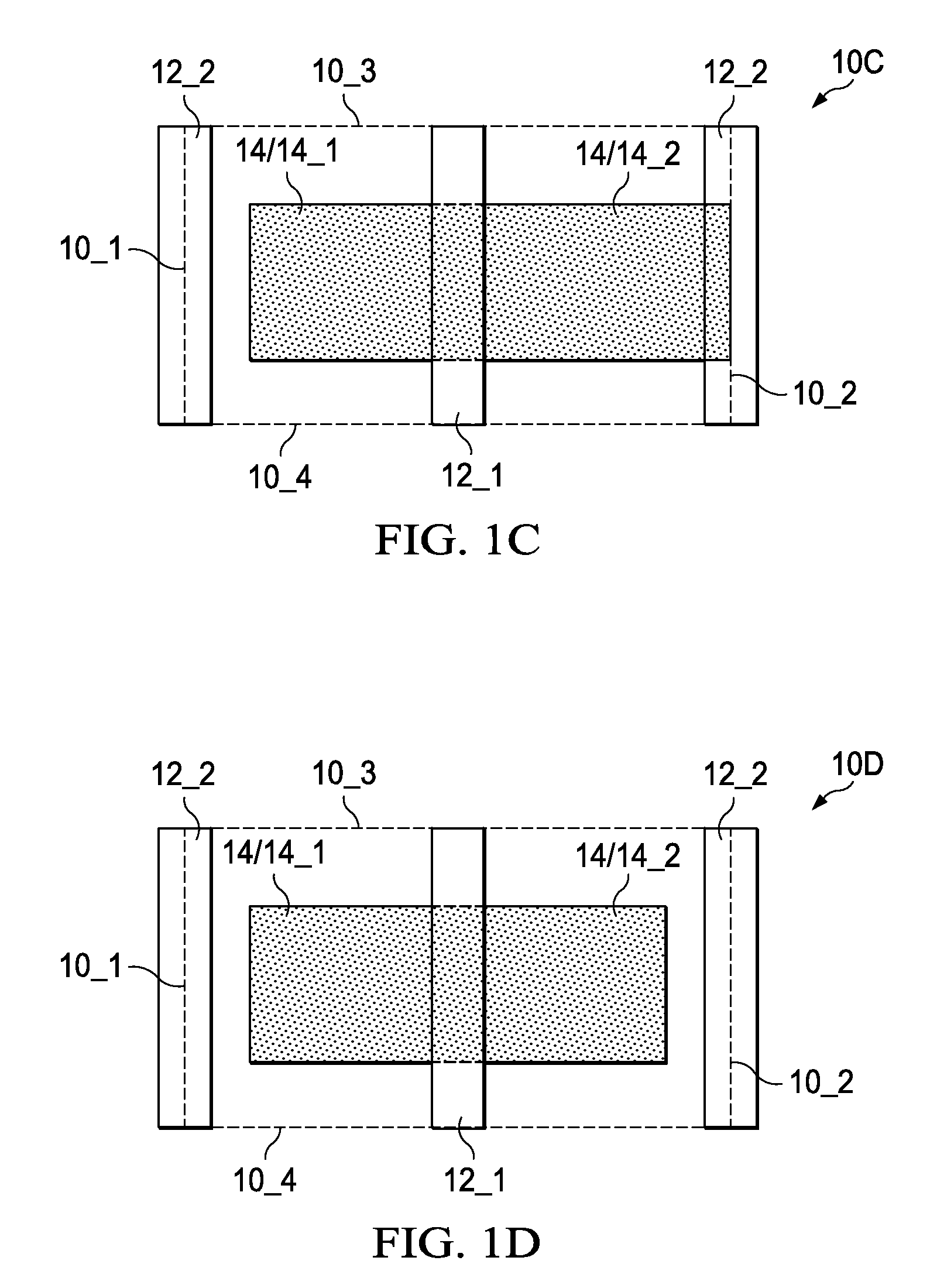
[0013]FIGS. 1A through 1D schematically illustrate the layouts (top views) of standard cells of different DFM types. It is to be noted that altho...


PUM


Abstract

Integrated circuit libraries include a first standard cell having a first left boundary and a first right boundary, and a second standard cell having a second left boundary and a second right boundary. The first standard cell and the second standard cell are of a same cell variant. A first active region in the first standard cell has a different length of diffusion than a second active region in the second standard cell. The first active region and the second active region are corresponding active regions represented by a same component of a same circuit diagram representing both the first standard cell and the second standard cell.

Description

[0001]This application claims the benefit of U.S. Provisional Application No. 61 / 174,352 filed on Apr. 30, 2009, entitled “Integrated Circuit Design using DFM-Enhanced Architecture,” which application is hereby incorporated herein by reference.TECHNICAL FIELD[0002]This invention relates generally to integrated circuit design, and more particularly to design-for-manufacturing (DFM) aware standard cell libraries, and to the methods for designing integrated circuits using the DFM aware standard cell libraries.BACKGROUND[0003]Conventionally, in the design of digital circuits, particularly application-specific integrated circuits (ASIC), standard cells are often pre-designed and saved in cell libraries. At the time integrated circuits (applications) are designed, the standard cells are retrieved from the cell libraries, and placed to desirable locations. Routing is then performed to connect the standard cells with each other, and with other customized circuits on the same chip.[0004]With...

Claims


Application Information

Patent Timeline
IPC IPC(8): G06F17/50
CPCG06F2217/12G06F17/5068G06F30/39G06F2119/18Y02P90/02
Inventor HOU, YUNG-CHINLU, LEE-CHUNGTIEN, LI-CHUNCHENG, YI-KANTAI, CHUN-HUIGUO, TA-PENHOU, YUAN-TE
Owner TAIWAN SEMICON MFG CO LTD
Learn More