Apparatus and method for low noise imaging

Active Publication Date: 2010-11-11
NUVU CAMERAS
View PDF9 Cites 7 Cited by
  • Summary
  • Abstract
  • Description
  • Claims
  • Application Information

AI Technical Summary

Benefits of technology

[0007]In an exemplary embodiment, the clock signal is substantially a sinusoid, but any other shape may be selected as desired to optimize the sensor readout with regard to readout time and noise minimization. For example, one alternative embodiment provides clock signal waveforms that compensate for interphase capacitance effects between out-of-phase signals that are applied in close proximity to one another. In another embodiment, the rise time of the clock waveforms applied, respectively, to adjacent charge positions is chosen to minimize the slope of the effective potential encountered by the electrons moving from one of said charge positions to an adjacent position.
[0008]The user-variable nature of the clock signals, such as the ability to vary the signal waveform shape and/or rise time, provi

Problems solved by technology

Conventional CCDs have limitations in low light situations because of the relatively high noise band of these devices.
While EMCCDs are successful in boosting signal gain substantially fo

Method used


Image

  • Apparatus and method for low noise imaging
  • Apparatus and method for low noise imaging
  • Apparatus and method for low noise imaging

Examples


Example

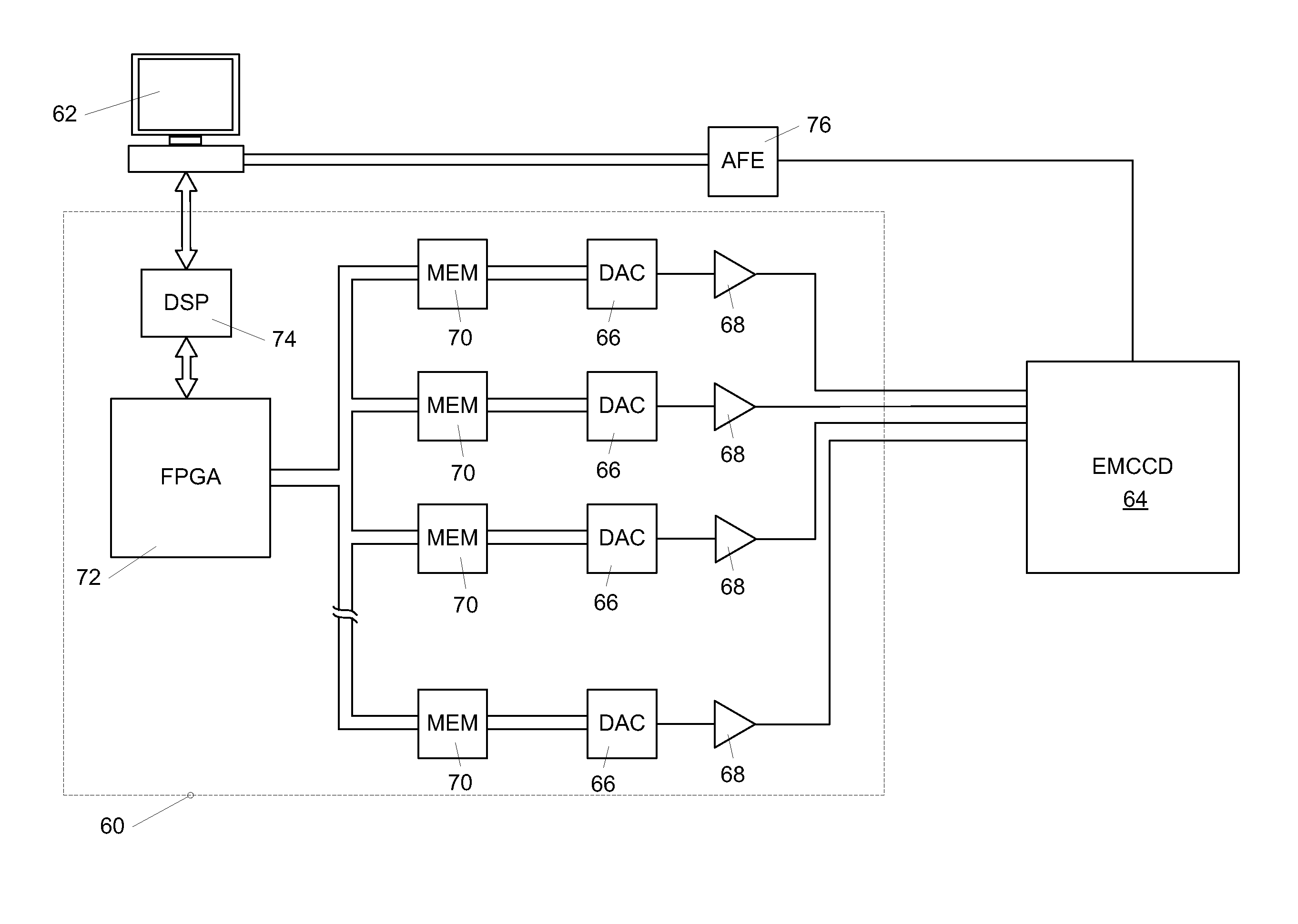
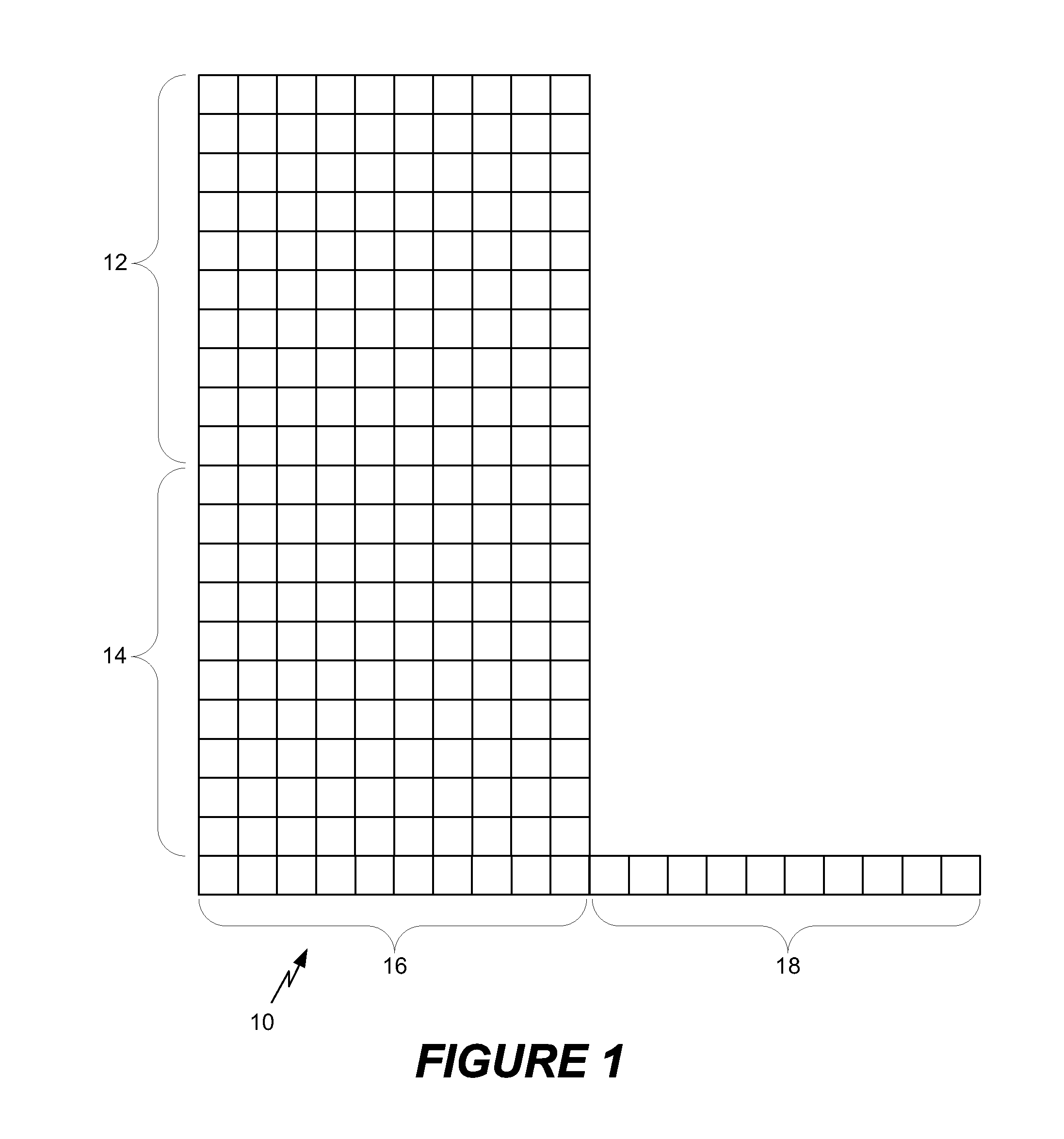
[0019]Shown in FIG. 1 is a schematic depiction of an EMCCD module 10 having two general regions, an image capture region 12 and a storage region 14. The module 10 is depicted as a grid of regions indicative of “pixels” or discrete image capture locations, although those skilled in the art will understand that the appearance of the module itself and the shape of the pixels will differ, and that the actual number of pixels used will be much higher. In addition, this is just one example of an imaging module, and other types exist that have different configurations but nonetheless function with the present invention, such as an EMCCD module having a capture region with no separate storage region. As is known in the art, the EMCCD module 10 may be used to capture an image in the region 12, each of the pixel locations accumulating photoelectrons, the total number of which is indicative of the amount of light received at that location. The image is captured during a predetermined exposure ...


PUM


Abstract

An apparatus and method for low noise imaging uses an image sensor, such as an EMCCD in which charges are accumulated and shifted out using analog clock signals. A sensor controller generates the clock signals from digital waveforms stored in memory units that provide outputs to digital-to-analog converters that, in turn, convert the signals to analog form. The analog signals are then amplified and applied to the sensor. The specific waveforms are determined by a digital signal processor and stored in the memories, and the desired waveforms are read out the memories using addressing provided by a field-programmable gate array. The clock signals may be sinusoids, or may be more complex waveform shapes, and the waveform shapes may be varied by a user. The clock signal rise times may be made gradual so as to minimize noise contributions.

Description

BACKGROUND OF THE INVENTION[0001]Low light optical detection applications require very sensitive optical detectors with relatively low noise in order to produce discernible signal outputs. In recent years, a popular type of imaging camera is based on the use of a so-called “electron multiplying charge coupled device” (EMCCD). A charge coupled device (CCD) is an analog shift register that allows electrical charges accumulated at individual locations, or pixels, in the CCD to be shifted from one charge position to an adjacent position. Such a device may be used in an optical imaging application by converting light arriving at each pixel location to photoelectrons. The accumulated electron charges at each of the pixel locations may then be “read out” of the CCD by progressive shifting from one position to the next. For a two-dimensional detector, the shifting is done in each of two perpendicular directions (referred to as “horizontal” and “vertical”).[0002]Conventional CCDs have limita...

Claims


Application Information

Patent Timeline
IPC IPC(8): H04N5/335
CPCH01L27/14609H04N5/378H04N5/3765H04N5/3577H04N25/617H04N25/745H04N25/75
Inventor DAIGLE, OLIVIER
Owner NUVU CAMERAS
Why Eureka
Try Eureka