Light emitter

Inactive Publication Date: 2010-11-18
E E JAPAN
View PDF0 Cites 41 Cited by
  • Summary
  • Abstract
  • Description
  • Claims
  • Application Information

AI Technical Summary

Benefits of technology

[0010]In the LED of the invention, the convex solid transparent resin projections are formed in the sealing resin surface; therefore, the LED has the following advantage: the light output efficiency is improved an

Problems solved by technology

These methods are not preferred since the methods

Method used


Image

  • Light emitter
  • Light emitter
  • Light emitter

Examples


example 1

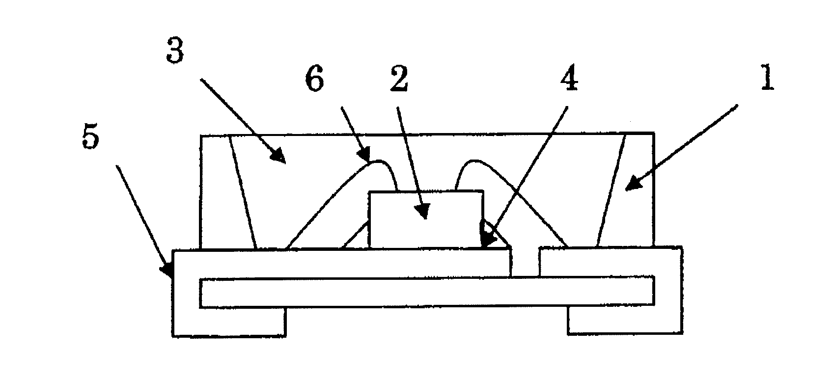
[0034]By an MOCVD epitaxial growing method, the following was formed on a C-surface sapphire substrate: a wafer which had a light emitting structure having a light emitting layer of InGaN and giving a dominant wavelength of 460 nm. The sapphire substrate was then polished into a thickness of about 100 μm. The wafer was then cut by a scribing method to form blue LED chips each having a size of 0.35 mm×0.35 mm. Next, prepared was a lead frame on which many packages in which of each a reflecting case was formed by injection mold were put, and the blue LED chips were die-bonded into the packages on the lead frame by a die-bonding agent made of a silicone resin. The agent was then cured. Thereafter, gold lines each having a diameter of 25 μm were used to carry out wire bonding on the anode side and the cathode side.

[0035]As a silicone resin of a sealing resin, a resin SRC 1011 manufactured by Shin-Etsu Chemical Co., Ltd was used. The specific gravity of this resin was 1.1×10³ kg / m3. As p...

example 2

[0037]An LED was formed in the same way as in Example 1 except that the plastic balls the particle diameter of which was changed to 10 μm were used in a proportion of 3% by weight in Example 1. The light output of the LED was measured. As a result, the light output was 15% better than that of an LED wherein no plastic balls were used.

example 3

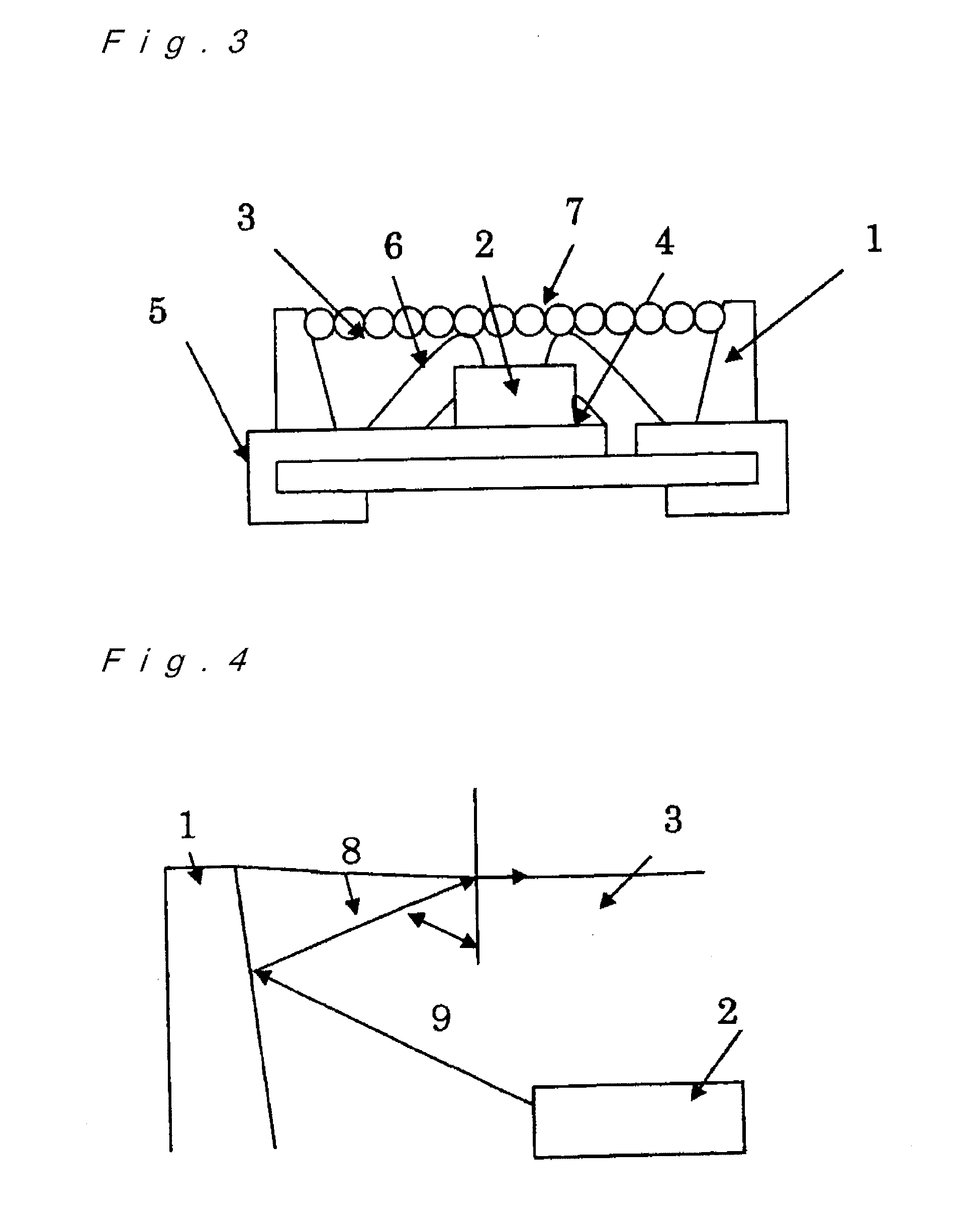
[0038]By an MOCVD epitaxial growing method, the following was formed on a C-surface sapphire substrate: a wafer which had a light emitting structure having a light emitting layer of InGaN and giving a dominant wavelength of 460 nm. The sapphire substrate was then polished into a thickness of about 100 μm. The wafer was then cut by a scribing method to form blue LED chips each having a size of 0.35 mm×0.35 mm. Next, prepared was a lead frame on which many packages in which of each a reflecting case was formed by injection mold were put, and the blue LED chips were die-bonded into the packages on the lead frame by a die-bonding agent made of a silicone resin. The agent was then cured. Thereafter, gold lines each having a diameter of 25 μm were used to carry out wire bonding on the anode side and the cathode side. The size of the opening in each of the packages, that is, the upper end size of each of the reflecting cases was 0.7 mm×0.7 mm.

[0039]As a solid transparent resin, plastic bal...


PUM


Abstract

The invention relates to a light emitter, such as an LED sealed with a resin, in particular, an LED wherein irregularities in a surface of a sealing resin can be formed through a simpler process in order to improve the light output efficiency of the LED. The LED is an LED wherein a liquid sealing resin is mixed with a solid transparent resin different from the sealing resin in specific gravity and subsequently the mixture is injected into a package into which an LED chip is integrated and then cured, thereby sealing the chip, characterized in that the solid transparent resin is fixed to the sealing resin to be partially naked to the sealing-resin-side surface of the LED through which light from the LED chip is emitted to the outside, and be partially embedded in the sealing resin, thereby being projected into the form of convexes. This LED is used for an LED displayer, an LCD backlight source, a lighting device or the like.

Description

TECHNICAL FIELD[0001]The present invention relates to a light emitter used for a light emitting diode displayer, an LCD backlight source, a lighting device or the like, and relates in particular to a structure for improving the light output efficiency of a light emitter, such as a light emitting diode sealed with a resin.BACKGROUND ART[0002]Light emitting diodes (hereinafter referred to as LEDs), organic or inorganic ELs, and other devices exist as light emitters. A typical structure of a displayer, an LCD backlight or an LED for lighting, among these devices, is illustrated in FIG. 1. This is the following structure: a structure wherein a silver paste or silicone resin die-bonding agent 4 is used to die-bond an LED chip 2 onto external metal electrodes 5 inside a package having a reflecting case 1 made of a plastic or ceramic material to give a good reflectivity; the die-bonding agent 4 is cured so as to bond positive and negative electrodes of the LED chip to the external electrod...

Claims


Application Information

Patent Timeline
IPC IPC(8): H01L33/56H01L33/58H01L33/48
CPCH01L33/486H01L33/54H01L33/56H01L2224/48091H01L2224/48247H01L2924/1815H01L2933/0091H01L2224/73265H01L2224/45144H01L2224/32225H01L2924/00014H01L2924/00
Inventor KUMURA, MASAO
Owner E E JAPAN
Why Eureka
Try Eureka