Semi-adaptive voltage scaling for low-energy digital vlsi-design

a digital vlsi design and digital vlsi technology, applied in the direction of resistance welding apparatus, welding electric supply, electric variable regulation, etc., can solve the problems of low efficiency, low efficiency, and low ideal minimum supply voltage, and achieve high efficiency, high complexity, and advantageously reduced power consumption of circuitry

Inactive Publication Date: 2010-11-18
ST ERICSSON SA
View PDF7 Cites 22 Cited by
  • Summary
  • Abstract
  • Description
  • Claims
  • Application Information

AI Technical Summary

Benefits of technology

[0071]An embodiment has a closed-loop mode during a production test phase of an electronic circuitry and an open-loop mode in an application phase, i.e., in operation, of the circuitry. During the production test, a lowermost level of the supply voltage is determined for the semiconductor circuitry at one single defined temperature, at which supply voltage all operating specifications of the circuit are fully met. The lowermost voltage level is stored in the electronic circuitry, e.g., in a dedicated electronic memory, together with temperature dependent parameters. Afterwards, in operation of the electronic circuitry, i.e., in a “real” application such as a mobile electronic device such as a mobile phone, personal digital assistant, laptop and so on, t

Problems solved by technology

However, the ideal minimal supply voltage is not known beforehand and differs from device to device.
Moreover, the calibration procedure must be done at these two predefined temperatures: Firstly, at a lower and at a higher temperature, which causes time delay

Method used


Image

  • Semi-adaptive voltage scaling for low-energy digital vlsi-design
  • Semi-adaptive voltage scaling for low-energy digital vlsi-design
  • Semi-adaptive voltage scaling for low-energy digital vlsi-design

Examples


Embodiment Construction

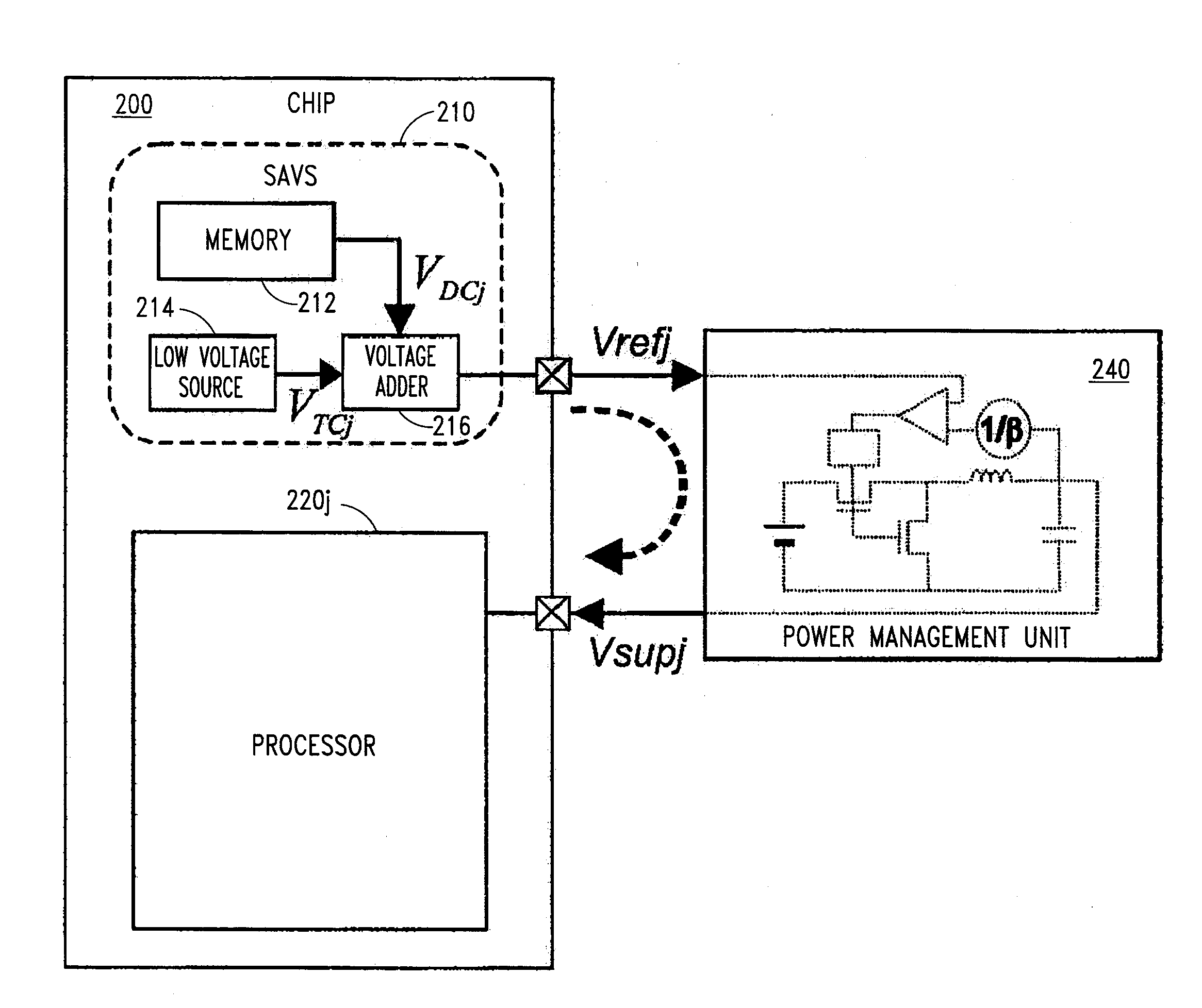
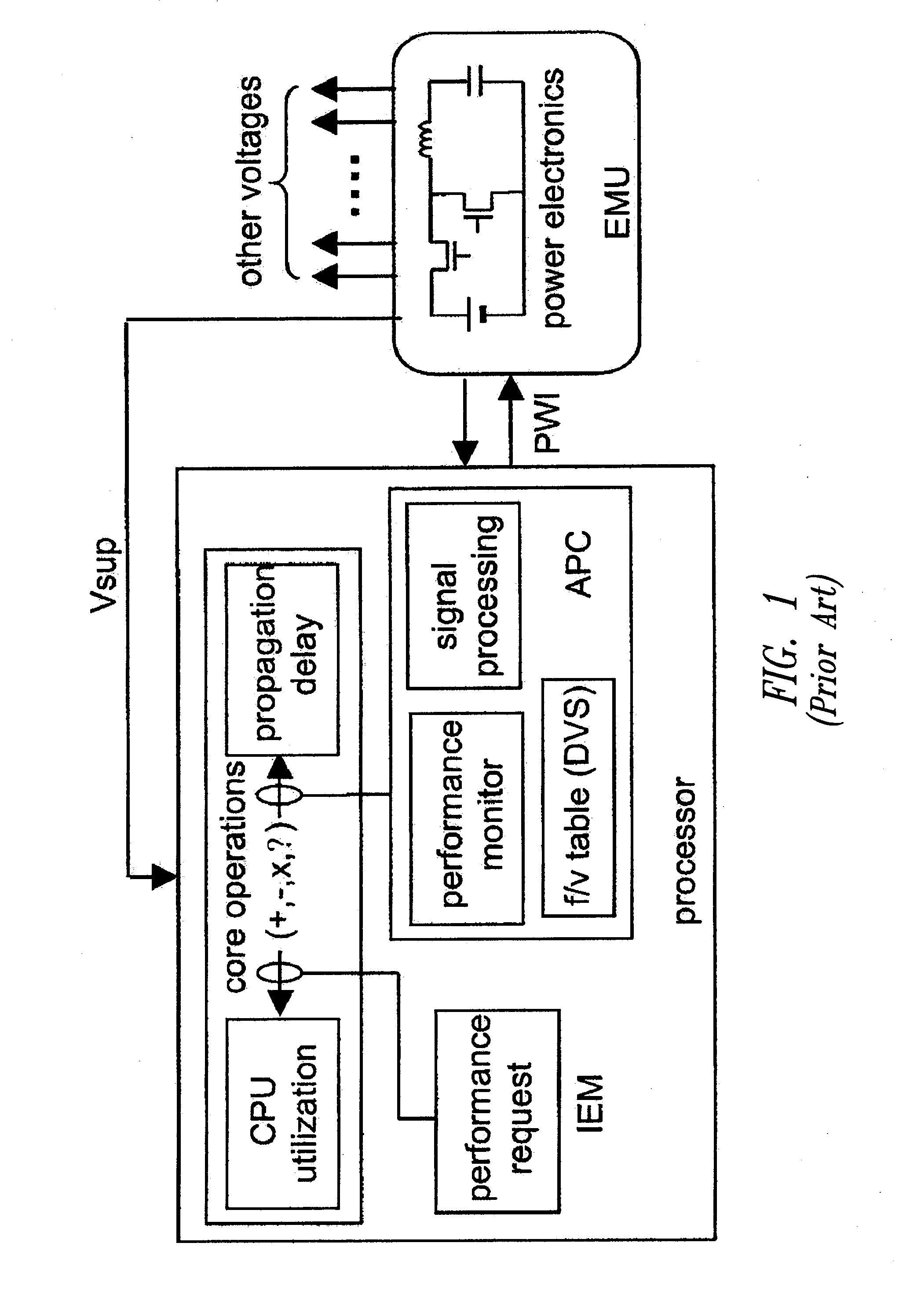
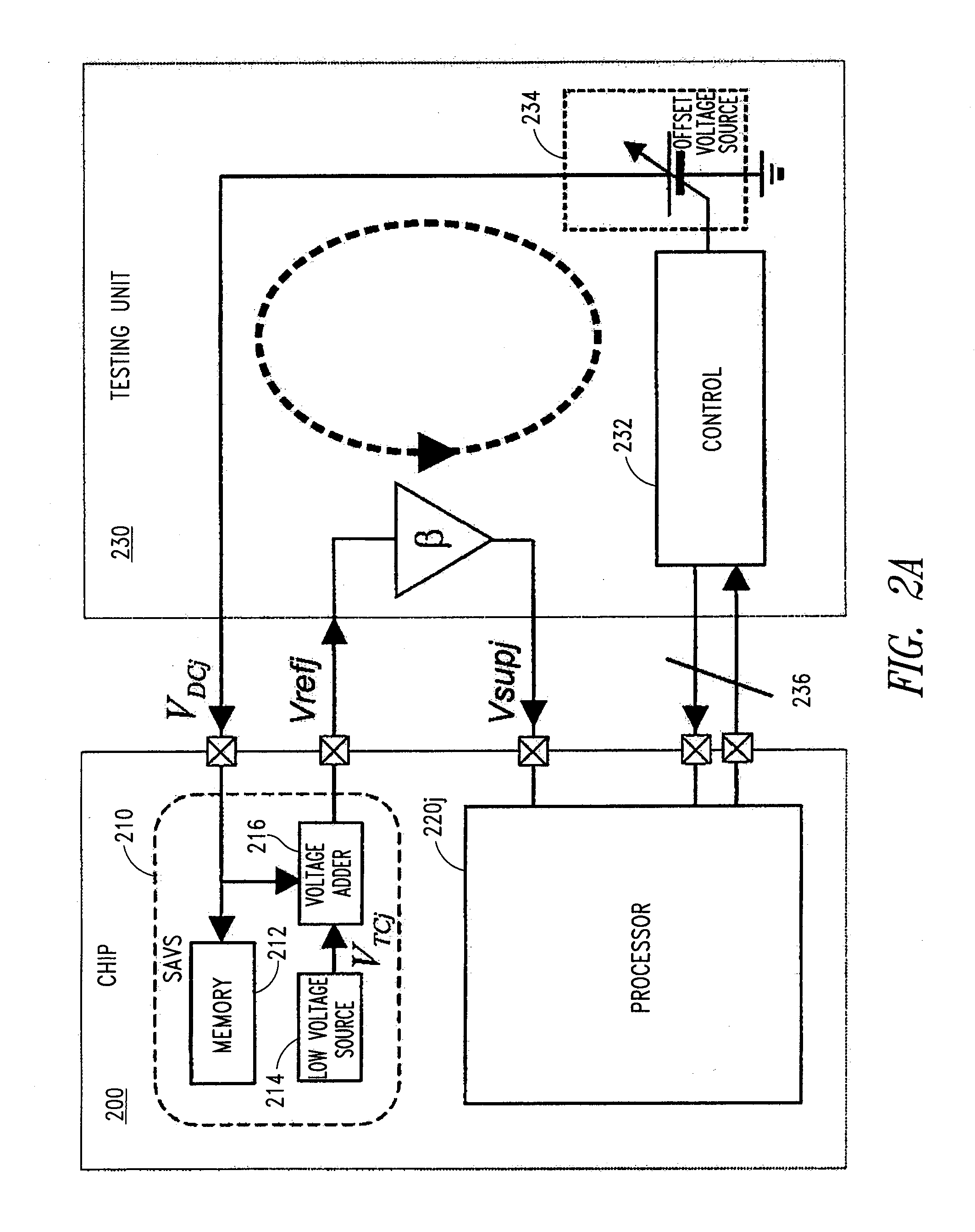
[0099]In the following description, numerous specific details are given to provide a thorough understanding of embodiments. The embodiments can be practiced without one or more of the specific details, or with other methods, components, materials, etc. In other instances, well-known structures, materials, or operations are not shown or described in detail to avoid obscuring aspects of the embodiments.

[0100]Reference throughout this specification to “one embodiment” or “an embodiment” means that a particular feature, structure, or characteristic described in connection with the embodiment is included in at least one embodiment. Thus, the appearances of the phrases “in one embodiment”“according to an embodiment” or “in an embodiment” and similar phrases in various places throughout this specification are not necessarily all referring to the same embodiment. Furthermore, the particular features, structures, or characteristics may be combined in any suitable manner in one or more embodi...


PUM

PropertyMeasurementUnit
Temperatureaaaaaaaaaa
Ratioaaaaaaaaaa
Electric potential / voltageaaaaaaaaaa

Abstract

A semi-adaptive voltage scaling method and device for determining minimal supply voltages for digital electronic semiconductor circuitry, e.g., microprocessors, of electronic devices under production testing and “real” operating conditions. The SAVS operates in a closed-loop during a production test phase of the circuitry and in an open-loop mode in an application (operation) phase of the semiconductor circuitry. During production testing, a lowermost level of the supply voltage for the semiconductor circuitry is determined at one single defined temperature at which operating specifications of the circuit are met. The lowermost level is stored in a dedicated electronic memory of the circuitry together with temperature dependent parameters. Afterwards, when the digital electronic circuitry is operated in a “real” application, e.g., a mobile phone, the device and method reads the previously measured and proven data from the memory and regenerates the minimum level of supply voltage for the circuitry, taking into account the actual temperature of the application. As a result, the digital semiconductor circuitry in the “real” application is supplied with a minimum level of supply voltage, whereby specified parameters of the circuitry are met. Thus, a power consumption of the circuitry is advantageously reduced to a minimum.

Description

BACKGROUND[0001]1. Technical Field[0002]The present disclosure relates to a method, a system, and a device with regard to supply voltages for individual digital electronic devices, such as microprocessors.[0003]2. Description of the Related Art[0004]As communication terminals are becoming more sophisticated and feature rich, energy consumption is increasing significantly. Hence, low-energy circuit design has become more important than ever before.[0005]Top-down analysis of cellular phone energy budget reveals that the digital circuitry typically consumes more than one third of the total energy of a cellular phone. Therefore, reducing energy consumption of digital circuits can contribute to overall energy reduction of cellular handsets. The energy consumed by digital circuitry can be divided into three components: dynamic energy, static energy, and short-circuit energy.[0006]In operation the short-circuit energy of properly designed digital circuits is negligible compared to dynamic ...

Claims


Application Information

Patent Timeline
IPC IPC(8): H02J4/00H01L21/66G05F1/10
CPCG01R31/31721
Inventor WANG, ZHENHUA
Owner ST ERICSSON SA
Why Eureka
Try Eureka