
Textured-surface light emitting diode and method of manufacture

a light-emitting diode and textured surface technology, applied in the field of optical techniques, can solve the problems of affecting the internal quantum efficiency, and affecting the efficiency of leds in part, and achieve the effect of high quality and high quality

Inactive Publication Date: 2010-11-25
SORAA +1
View PDF107 Cites 106 Cited by
  • Summary
  • Abstract
  • Description
  • Claims
  • Application Information

AI Technical Summary

Benefits of technology

[0011]In a specific embodiment, the present invention provides a method of making a light emitting diode. The method includes providing a high quality nitride crystal comprising a base nitride crystal and an overlying release layer. In a specific embodiment, the high quality nitride crystal comprises a gallium species and a nitrogen species and having a surface dislocation density below 105 cm−2. The method forms an n-type semiconductor layer comprising a gallium species and nitrogen species overlying the release layer and a semiconductor active layer comprising a gallium species and a nitrogen species. In a specific embodiment, the semiconductor active layer is characterized by a peak light emission wavelength, and a p-type semiconductor layer comprising a gallium species and a nitrogen species overlying the high quality nitride crystal to form a sandwiched structure. In a specific embodiment, the method forms a reflective metallic contact overlying the p-type semiconductor layer. In a specific embodiment, the present method also separates the base nitride crystal from the sandwiched structure to expose a portion of the n-type layer. The method also processes, using at least etching, at least half of the exposed portion of the n-type layer to form one or more pyramidal structures, with side angles of between about 10 degrees and about 90 degrees with respect to the exposed portion of the n-type layer. The one or more pyramidal structures has a characteristic length scale between about 10 nm and about 1000 nm.
[0012]In an alternative specific embodiment, the present invention provides a light emitting diode device. The device includes a semiconductor active layer comprising a gallium species and a nitrogen species. The semiconductor active layer is characterized by a peak emission wavelength. The device also has a semiconductor n-type layer comprising a gallium species and a nitrogen species underlying the semiconductor active layer. The device has a semiconductor p-type layer comprising a gallium species and a nitrogen species overlying the semiconductor active layer and an electrical contact coupled to one or more portions of the semiconductor n-type layer. The device has a reflective electrical contact coupled to at least one of the semiconductor p-type layer or the semiconductor n-type layer and an active layer surface dislocation density below about 105 cm−2 characterizing the active layer. The device has an n-type layer surface dislocation density below about 105 cm−2 characterizing the n-type layer and a p-type layer surface dislocation density below about 105 cm−2 characterizing the p-type layer. In a specific embodiment, the device has one or more pyramidal structures texturing at least half of a surface region of at least one of the n-type layer or p-type layer. The one or more pyramidal structures has a plurality of pyramidal angles of between about 10 degrees and about 90 degrees with respect to the surface region and the one or more pyramidal structures has a characteristic length scale between about 10 nm and about 1000 nm.

Problems solved by technology

The efficiency of LEDs is limited in part by the internal quantum efficiency and by the light extraction efficiency.
However, this approach suffers from several limitations.
The use of a sapphire or other non-GaN substrate, while providing a means for removal of the substrate, does not achieve low dislocation densities in the active layer, which may negatively impact the internal quantum efficiency.
However, the '413 patent is generally limited to removal using lapping, polishing, chemical etching, plasma etching, and ion beam etching for removal of the substrate portion.
These methods do not appear to provide a natural endpoint, and it is therefore extremely difficult to remove all but a few- or sub-micron-thick layer of uniform thickness, and are slow and expensive to perform.

Method used


Image

  • Textured-surface light emitting diode and method of manufacture
  • Textured-surface light emitting diode and method of manufacture
  • Textured-surface light emitting diode and method of manufacture

Examples


Embodiment Construction

[0017]According to the present invention, optical techniques are provided. More specifically, embodiments of the invention include techniques for fabricating a light emitting diode device using bulk gallium nitride containing materials. Merely by way of example, the invention can be applied to applications such as optoelectronic devices, and the like. For clarity, and consistent with standard usage in the art, unless otherwise specified, the term “wavelength” as used herein refers to the wavelength of radiation propagating in air and may be donoted by the symbol λ.

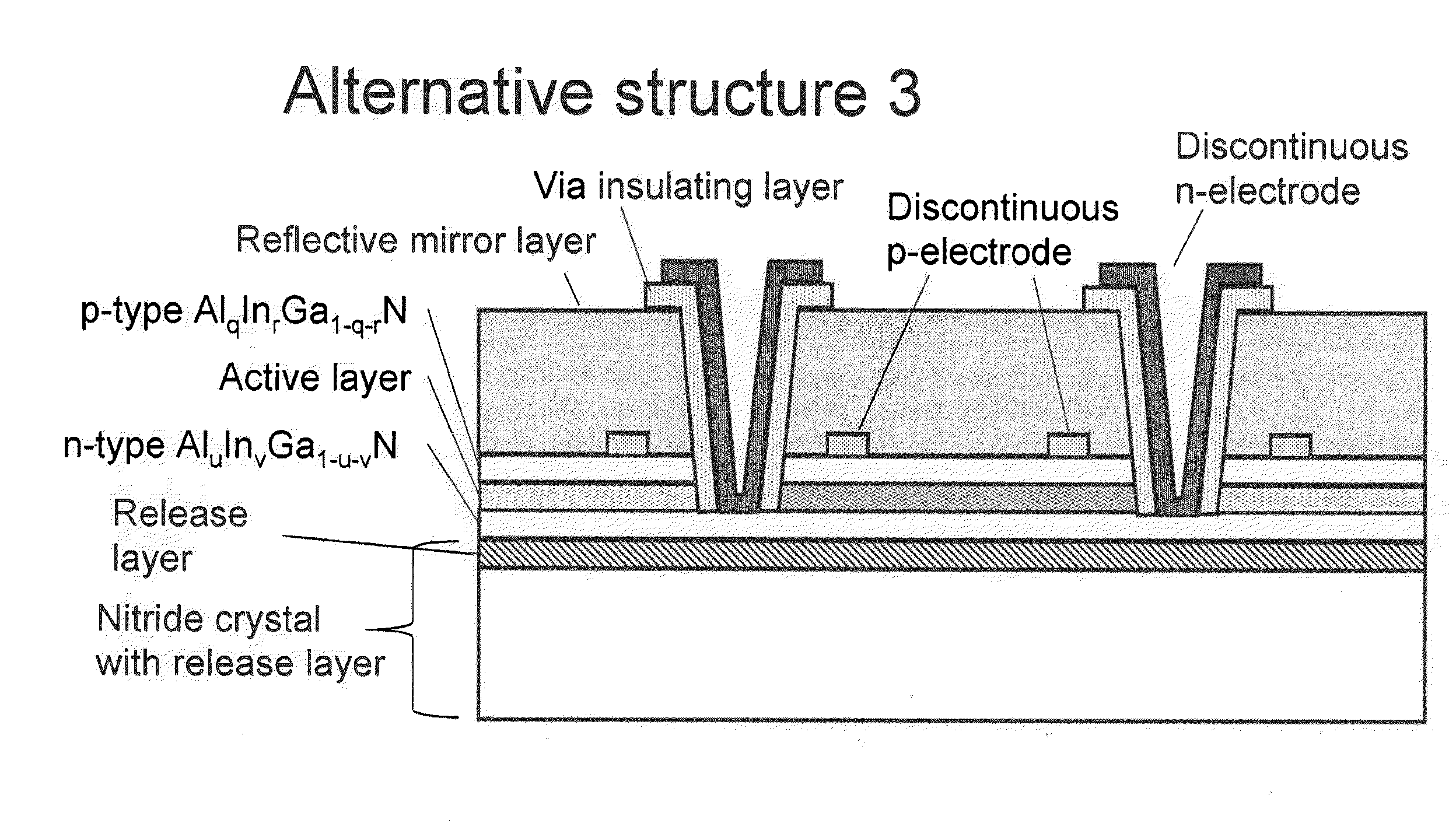
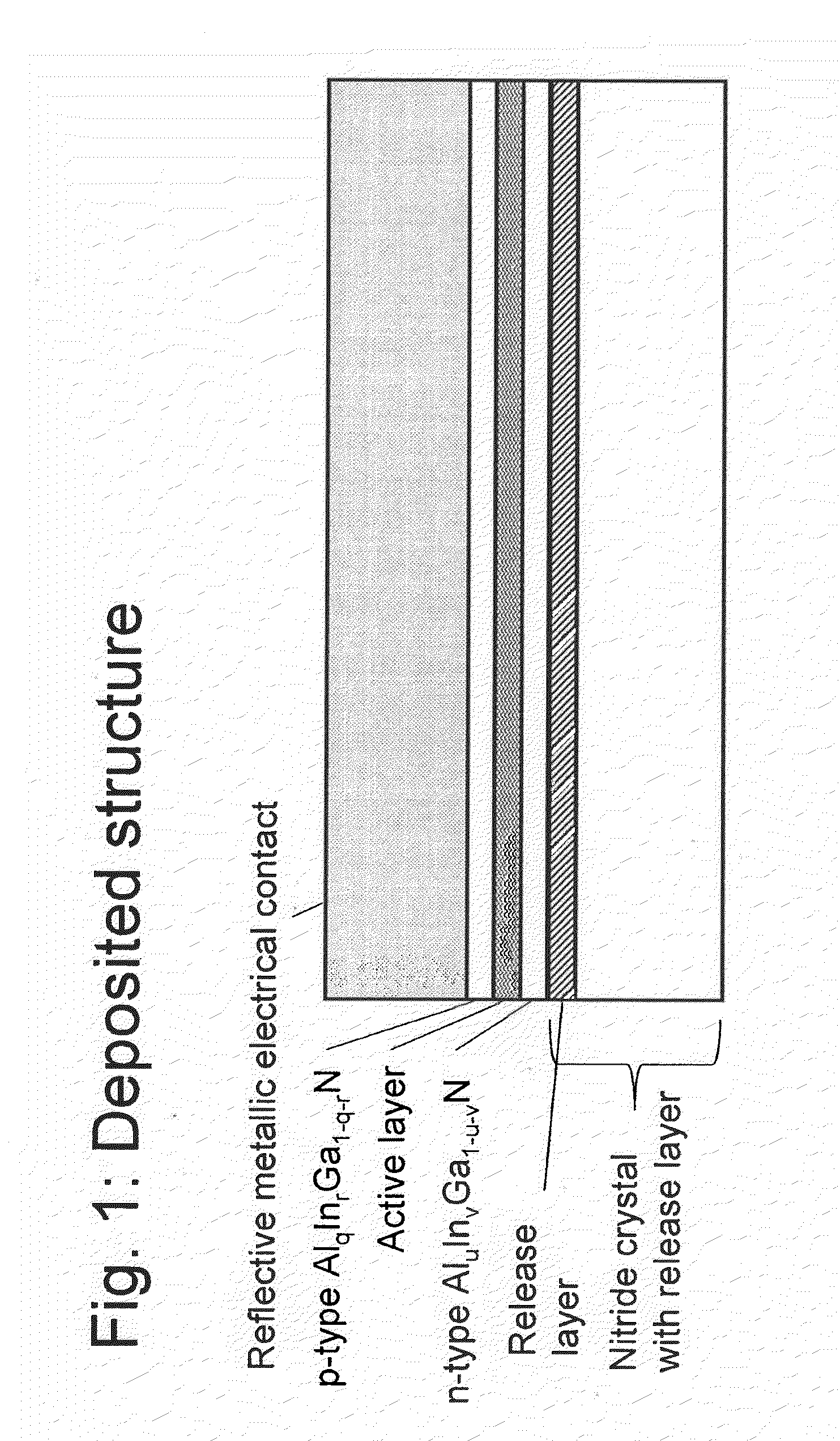
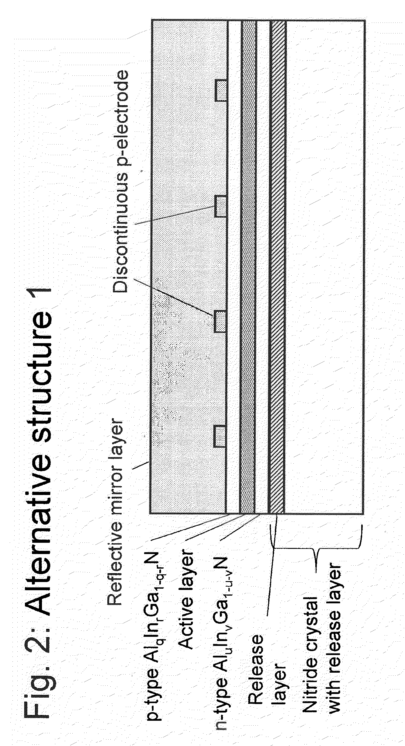
[0018]Referring to FIG. 1, the starting point for the present invention is a substrate consisting essentially of a high quality nitride crystal with a release layer, as disclosed in U.S. Patent application 61 / 091,591, entitled, “Nitride crystal with release layer, method of making, and method of use,” which is hereby incorporated by reference in its entirety. The nitride crystal comprises nitrogen and has a surface disloca...


PUM


Abstract

A high efficiency textured-surface light emitting diode comprises a flip-chipped stack of AlxInyGa1-x-yN layers, where 0≦x, y, x+y≦1. Each layer has a high crystalline quality, with a dislocation density below about 105 cm−2. The backside of the stack, exposed by removal of the original substrate, has a textured surface for improved light extraction.

Description

CROSS-REFERENCES TO RELATED APPLICATIONS[0001]This application claims priority to U.S. Provisional Patent Application No. 61 / 102,347 filed Oct. 2, 2008, commonly assigned, and of which is incorporated in its entirety by reference herein for all purposes.STATEMENT AS TO RIGHTS TO INVENTIONS MADE UNDER FEDERALLY SPONSORED RESEARCH AND DEVELOPMENT[0002]Not ApplicableREFERENCE TO A “SEQUENCE LISTING,” A TABLE, OR A COMPUTER PROGRAM LISTING APPENDIX SUBMITTED ON A COMPACT DISK[0003]Not ApplicableBACKGROUND OF THE INVENTION[0004]The present invention relates generally to optical techniques. More specifically, embodiments of the invention include techniques for fabricating a light emitting diode device using bulk gallium nitride containing materials. Merely by way of example, the invention can be applied to applications such as optoelectronic devices, and the like.[0005]Much progress has been made during the past decade and a half in the performance of gallium nitride (GaN) based light emi...

Claims


Application Information

Patent Timeline
Patent Type & Authority Applications(United States)
IPC IPC(8): H01L33/62
CPCH01L33/0079H01L33/18H01L33/405H01L33/382H01L33/32H01L33/0093
Inventor D'EVELYN, MARK P.SHARMA, RAJATHALL, ERIC M.FEEZELL, DANIEL F.SCHMIDT, MATHEW C.
Owner SORAA
Features
  • Generate Ideas
  • Intellectual Property
  • Life Sciences
  • Materials
  • Tech Scout
  • Unparalleled Data Quality
  • Higher Quality Content
  • 60% Fewer Hallucinations
Learn More