Methods and systems for fabrication of MEMS CMOS devices

Inactive Publication Date: 2010-11-25
BAOLAB MICROSYST
View PDF30 Cites 96 Cited by
  • Summary
  • Abstract
  • Description
  • Claims
  • Application Information

AI Technical Summary

Benefits of technology

[0011]By more carefully controlling the vapor HF etching process, the present inventive techniques eliminate the need for additionally and more costly fabrication steps or modifications of the standard CMOS fabrication process. For example, a CMOS chip typically includes an inter dielectric layer (ILD) between the silicon substrate and the interconnect layers. To prevent excessive etching of the ILD or silicon substrate, an conductor layer (or conductive metal layer), which is resistant to vapor HF, can be positioned between the ILD and interconnect layers to prevent excessive etching by the vapor HF of the ILD and / or substrate. A conductor layer may be positioned above the MEMS component and include one or more holes, aligned above a MEMS component, that allow for the passage of vapor HF into one or more interconnect layers to effect the release of the MEMS component.
[0013]A top layer of the conductor material used to form the CMOS MEMS device may include one or more holes to allow the vapor HF to pass through, while inhibiting other gases or materials to pass through. Instead of having to position a hole or trench outside the area of the MEMS, the present application enables the one or more holes to be aligned above the MEMS because the vapor HF etching process can be controlled. Thus, enabling a more efficient and less intrusive post CMOS fabrication technique for releasing the MEMS as opposed to a two step process where hole must be formed outside the MEMS structure to enable line-of-site etching. More than one top conductor layer may also be used where each layer includes holes that are not aligned vertically. In this arrangement, when the holes are sealed, the offset arrangement of holes between layers inhibits the sealing material from reaching or affecting the MEMS.

Problems solved by technology

While others have developed various CMOS MEMS fabrication techniques, no one has realized a way to robustly and reliably fabricate a CMOS MEMS chip using vapor HF (vHF) to etch the MEMS component within the interconnect layers.
Unless the vapor HF etching process is carefully controlled, the etching process is susceptible to a run-away reaction where an excessive portion of a chip is etched and / or the MEMS component is damaged or destroyed.
Existing fabrication techniques do not address this problem and existing CMOS MEMS manufacturers have typically avoided using vapor HF for this reason.

Method used


Image

  • Methods and systems for fabrication of MEMS CMOS devices
  • Methods and systems for fabrication of MEMS CMOS devices
  • Methods and systems for fabrication of MEMS CMOS devices

Examples


Embodiment Construction

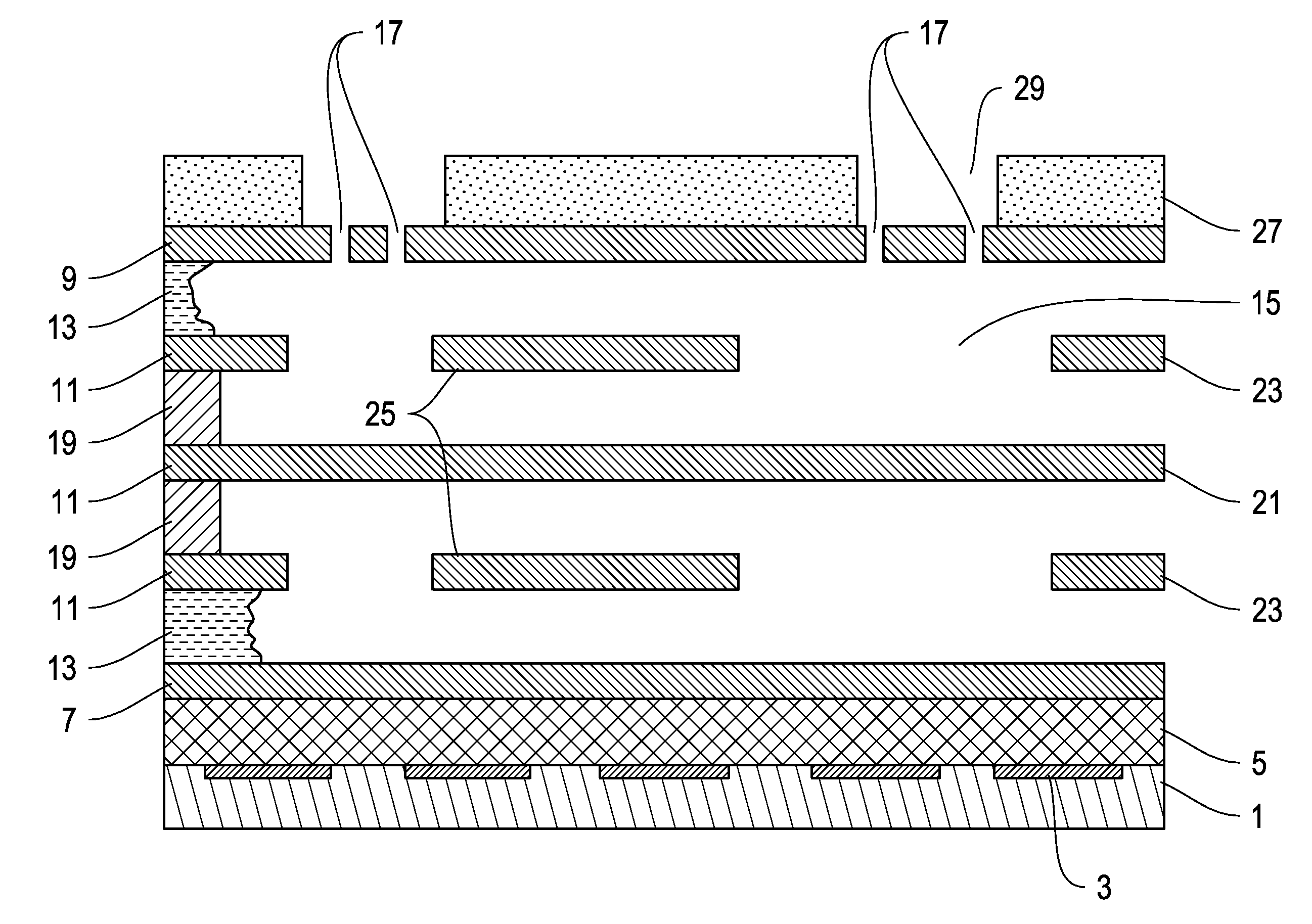
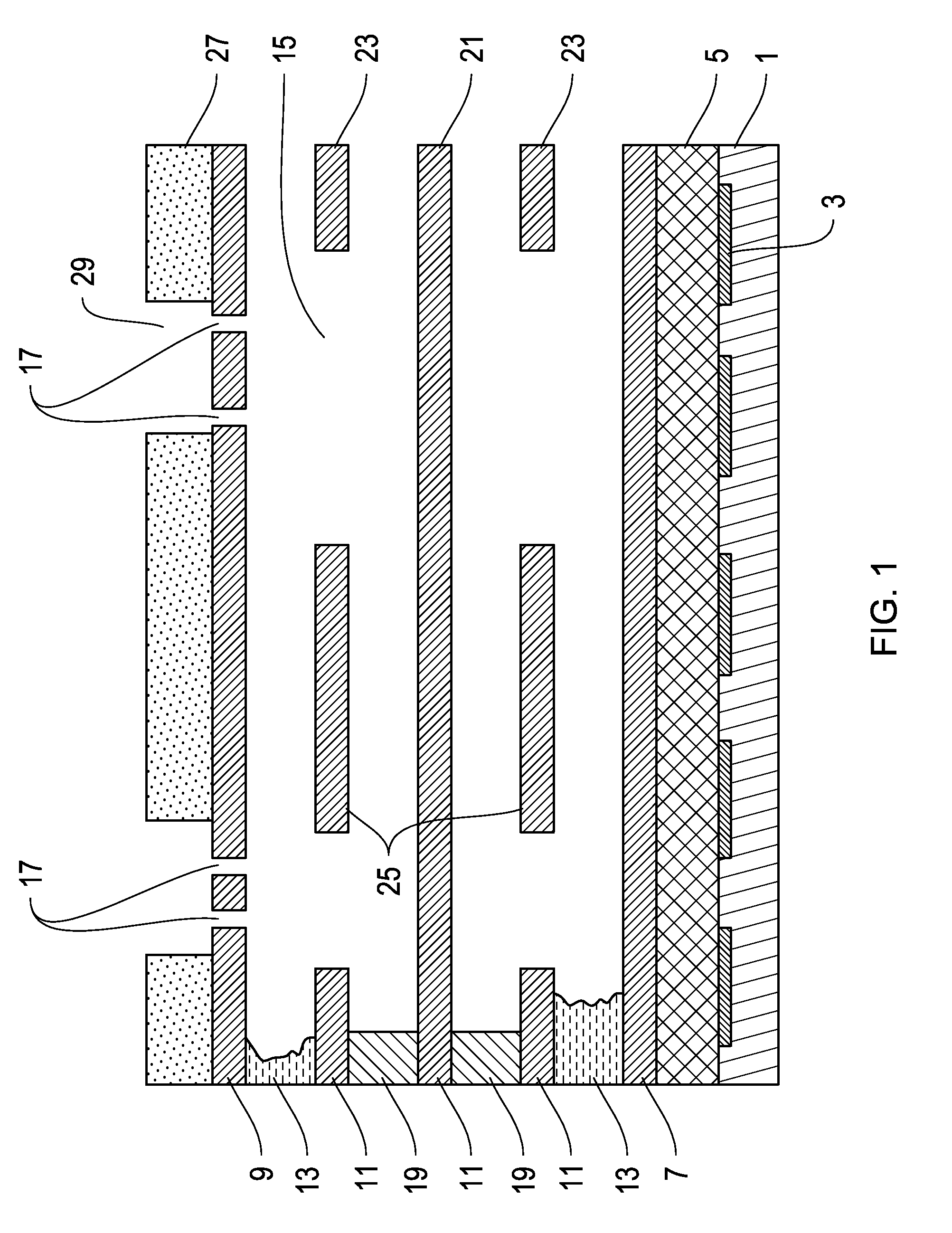
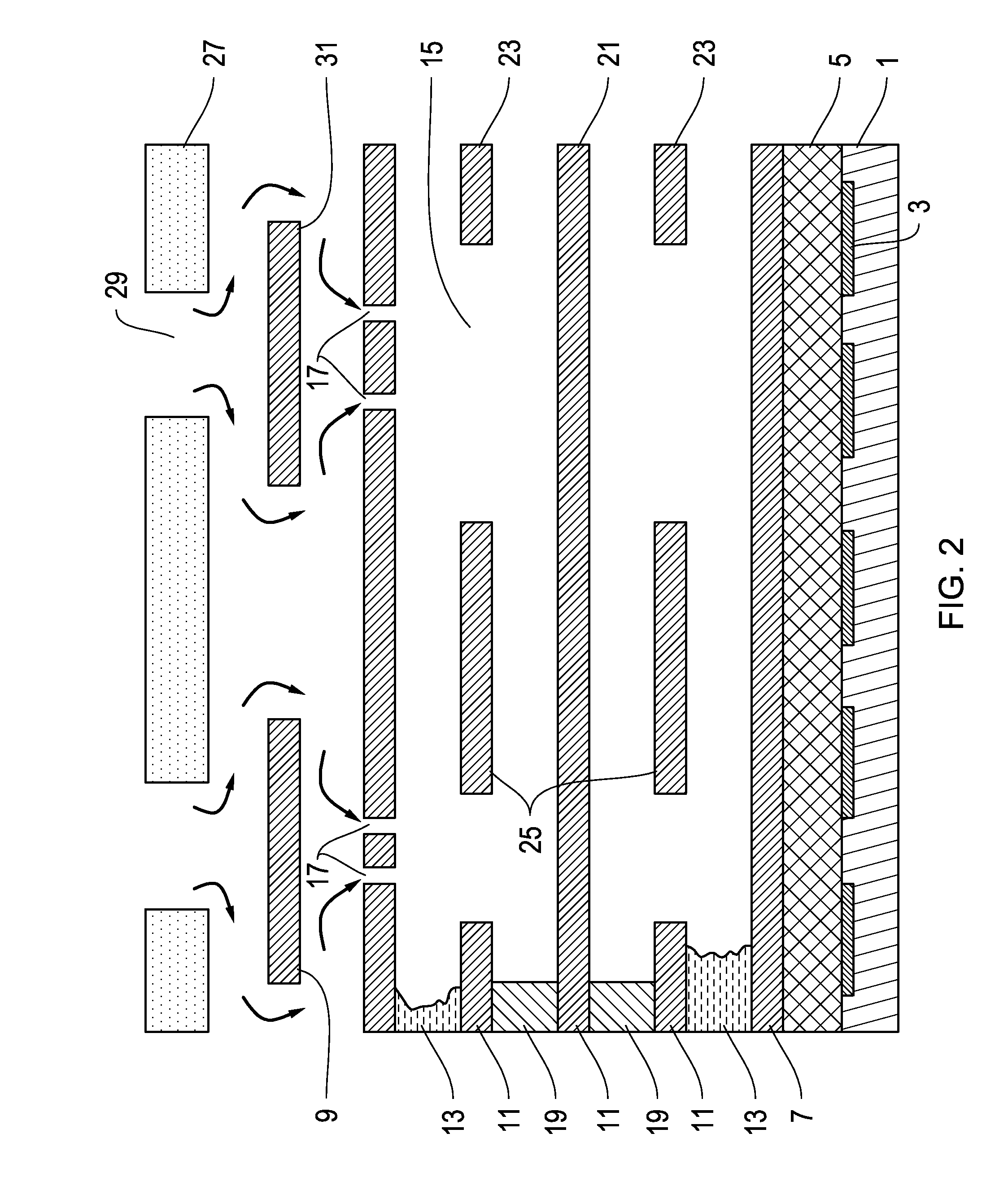
[0095]The application relates to a manufacturing method of a chip comprising a MEMS arranged in an integrated circuit, where the MEMS comprises at least one hollow space. The method comprising:

[0096]a) stages for producing layers that form electrical or electronic elements on a substrate made of semiconductor material, and

[0097]b) an interconnection stage, in which a structure of interconnection layers is made, which comprises depositing at least one bottom layer of conductor material and one top layer of conductor material separated by at least one layer of dielectric material.

[0098]The invention also relates to a chip comprising an integrated circuit, said integrated circuit comprising:

[0099]a) layers forming electrical or electronic elements on a substrate of semiconductor material,

[0100]b) a structure of interconnection layers, with at least one bottom layer of conductor material and one top layer of conductor material separated by at least one layer of dielectric material.

[0101...


PUM


Abstract

A MEMS integrated circuit including a plurality of layers where a portion includes one or more electronic elements on a semiconductor material substrate. The circuit includes a structure of interconnection layers having a bottom layer of conductor material and a top layer of conductor material where the layers are separated by at least one layer of dielectric material. The bottom layer may be formed above and in contact with an Inter Dielectric Layer. The circuit also includes a hollow space within the structure of interconnection layers and a MEMS device in communication with the structure of interconnection layers.

Description

CROSS REFERENCE TO RELATED APPLICATIONS[0001]This application claims priority to Spanish Patent Application No. P200901282 filed May 20, 2009, entitled “Chip Comprising a MEMS Arranged in an Integrated Circuit and Corresponding Manufacturing Method”, hereby incorporated by reference in its entirety. This application also claims priority to U.S. Provisional Patent Application No. 61 / 311,997 filed Mar. 9, 2010, entitled “Methods and Systems for Fabrication of MEMS CMOS Devices”; U.S. Provisional Patent Application No. 61 / 312,017 filed Mar. 9, 2010, entitled “MEMS CMOS Vibrating Antenna and Fabrication Thereof”; U.S. Provisional Patent Application No. 61 / 312,027 filed Mar. 9, 2010, entitled “MEMS CMOS Integrated Inductor and Fabrication Thereof”; and U.S. Provisional Patent Application No. 61 / 312,034 filed Mar. 9, 2010, entitled “MEMS CMOS Modal Switch and Fabrication Thereof”, hereby incorporated by reference in their entireties.BACKGROUND OF THE INVENTION[0002]An integrated circuit i...

Claims


Application Information

Patent Timeline
IPC IPC(8): H01L29/84H01L21/306
CPCB81C1/00246B81C2203/0145B81C2203/0714B81C2203/0771H01L21/31116H01L23/5223H01L28/40H01L2924/1461H01L2924/13091H01L24/05H01L2924/00H01L2924/351H01L2924/14H01L2224/05569H01L2224/05008B81B7/02H01L21/30
Inventor MONTANYA SILVESTRE, JOSEPVALLE FRAGA, JUAN JOSELLAMAS MOROTE, MARCO ANTONIOSABIR, TAYYIB
Owner BAOLAB MICROSYST
Why Eureka
Try Eureka