Array substrate for fringe field switching mode liquid crystal display device

a fringe field switching and liquid crystal display technology, applied in non-linear optics, instruments, optics, etc., can solve the problems of poor viewing angle of am-lcd devices, disadvantages of ips mode lcd devices in aperture ratio and transmissivity

Active Publication Date: 2010-11-25
LG DISPLAY CO LTD
View PDF4 Cites 59 Cited by
  • Summary
  • Abstract
  • Description
  • Claims
  • Application Information

AI Technical Summary

Problems solved by technology

However, since the AM-LCD device uses a vertical electric field, the AM-LCD device has a bad viewing angle.
Unfortunately, the IPS mode LCD device has disadvantages in an aperture ratio and transmissivity.
Unfortunately, the related art FFS mode LCD device has a mono-domain structure such that an azimuth angle is changed depending on a position of the user.

Method used


Image

  • Array substrate for fringe field switching mode liquid crystal display device
  • Array substrate for fringe field switching mode liquid crystal display device
  • Array substrate for fringe field switching mode liquid crystal display device

Examples


first embodiment

[0034]FIG. 4 is a plane view showing one pixel region of an array substrate for an FFS mode LCD device according to the present invention. For convenience of explanation, a region, where a plurality of pixel regions are defined, is defined as a display region, and a region at a periphery of the display region is defined as a non-display region. A switching region, where a TFT is formed, is defined in the pixel region.

[0035]In FIG. 4, a gate line 105 and a data line 130 are formed on a substrate 101 to define a pixel region “P”. In each pixel region “P”, a thin film transistor Tr as a switching element is formed. The TFT “Tr” is connected to the gate and data lines 105 and 130 and includes a gate electrode 108, a gate insulating layer (not shown), a semiconductor layer (not shown) including an active layer of intrinsic amorphous silicon and an ohmic contact layer of impurity-doped amorphous silicon, a source electrode 133 and a drain electrode 136. The drain electrode 136 is spaced a...

second embodiment

[0041]FIG. 5 is a plane view showing one pixel region of an array substrate for an FFS mode LCD device according to the present invention, and FIG. 6 is an enlarged view of an “A” portion of FIG. 5.

[0042]In FIGS. 5 and 6, a gate line 205 and a data line 230 are formed on a substrate 201 to define a pixel region “P”. In each pixel region “P”, a thin film transistor Tr as a switching element is formed. The TFT “Tr” is connected to the gate and data lines 205 and 230 and includes a gate electrode 208, a gate insulating layer (not shown), a semiconductor layer (not shown) including an active layer of intrinsic amorphous silicon and an ohmic contact layer of impurity-doped amorphous silicon, a source electrode 233 and a drain electrode 236. The drain electrode 236 is spaced apart from the source electrode 233 such that a portion of the active layer is exposed through the source and drain electrodes 233 and 236. As mentioned above, a shape of a channel region of the TFT “Tr” and a positio...

third embodiment

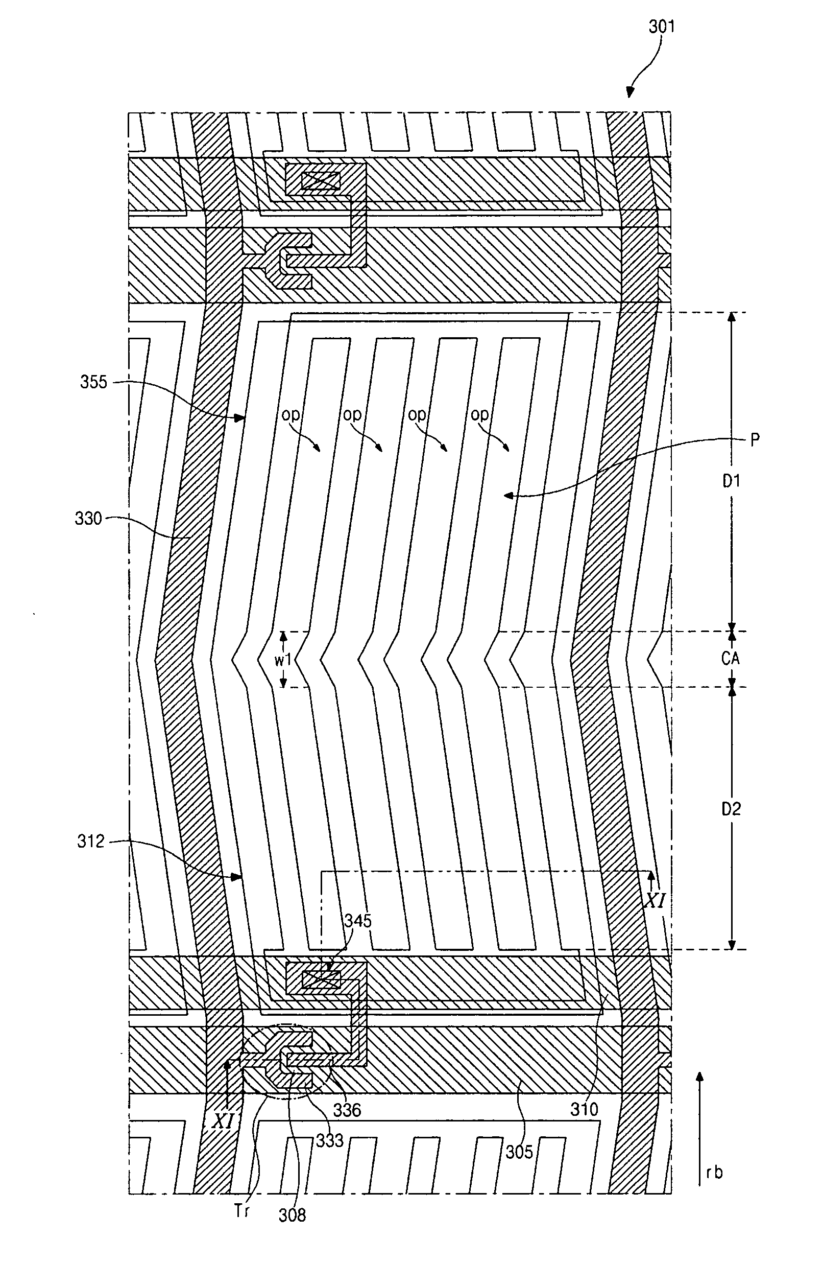
[0055]FIG. 9 is a plane view showing one pixel region of an array substrate for an FFS mode LCD device according to the present invention, and FIG. 10 is a cross-sectional view taken along the line XI-XI of FIG. 9.

[0056]As shown in FIGS. 9 and 10, the third embodiment has difference in shapes of a common and pixel electrodes 312 and 355, positions of the common and pixel electrodes 312 and 355 and a common line 310 from the second embodiment.

[0057]In FIGS. 9 and 10, a gate line 305 is formed on a substrate 301, and the common line 310 is formed on the substrate 301 to be spaced apart from and parallel to the gate line 301. The common electrode 312 having a plate shape is formed in each pixel region “P” and connected to the common line 310. The pixel electrode 355 including a plurality of openings “op” is positioned over the common electrode 312 and in each pixel region “P” with a gate insulating layer 315 and a passivation layer 340 interposed therebetween. The pixel electrode 355 i...


PUM

PropertyMeasurementUnit
angleaaaaaaaaaa
angleaaaaaaaaaa
vertical lengthaaaaaaaaaa

Abstract

An array substrate for a fringe field switching mode liquid crystal display device includes a substrate including a plurality of pixel regions each having a first domain, a second domain and a domain boundary area between the first and second domains; gate and data lines on the substrate and crossing each other to define the pixel region; a thin film transistor in each pixel region and connected to the gate and data lines; a pixel electrode in each pixel region and connected to the thin film transistor; and a common electrode overlapping the pixel electrode with an insulating layer interposed between the common and pixel electrode, wherein a plurality of openings are formed through the common electrode or the pixel electrode, and each opening has a first angle in the first and second domains with respect to a rubbing direction and a second angle larger than the first angle in the domain boundary area with respect to the rubbing direction.

Description

[0001]The present application claims the benefit of Korean Patent Application No. 10-2009-0044890 filed in Korea on May 22, 2009, which is hereby incorporated by reference for all purposes as if fully set forth herein.BACKGROUND OF THE INVENTION[0002]1. Field of the Invention[0003]The present invention relates to a liquid crystal display (LCD) device, and more particularly, to an array substrate for a fringe field switching (FFS) mode LCD device capable of having a multi-domain structure.[0004]2. Discussion of the Related Art[0005]A related art liquid crystal display (LCD) device uses optical anisotropy and polarization properties of liquid crystal molecules. The liquid crystal molecules have a definite alignment direction as a result of their thin and long shapes. The alignment direction of the liquid crystal molecules can be controlled by application of an electric field across the liquid crystal molecules. As the intensity or direction of the electric field is changed, the alignm...

Claims


Application Information

Patent Timeline
Patent Type & Authority Applications(United States)
IPC IPC(8): G02F1/1343
CPCG02F2001/134372G02F1/134363G02F1/134372G02F1/1343G02F1/1337
Inventor HAN, SANGHUNHEE, KYUNG-HAPARK, IN-CHEOL
Owner LG DISPLAY CO LTD
Why Eureka
Try Eureka