

Method for manufacturing semiconductor device, apparatus for manufacturing semiconductor device, program for manufacturing semiconductor device, and program for generating mask data
- Summary
- Abstract
- Description
- Claims
- Application Information
AI Technical Summary
Benefits of technology
Problems solved by technology
Method used
Image

Examples
ninth embodiments
2. Specific embodiments (first to ninth embodiments)
3. Form of program
1. Configuration in which the Present Embodiment is Applied Apparatus Configuration
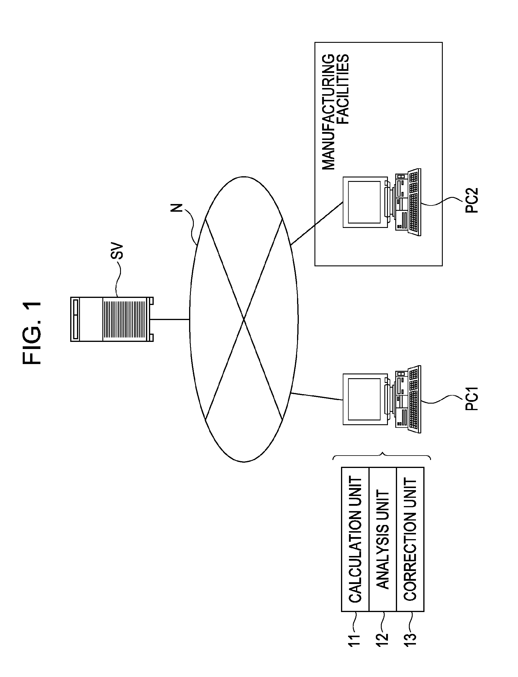
[0045]FIG. 1 illustrates an example of the configuration of a system to which an apparatus for manufacturing a semiconductor device according to the present embodiment is applied. The apparatus for manufacturing a semiconductor device according to the present embodiment is mainly realized using a computer PC1. The computer PC1 is connected to a network N. The computer PC1 reads various data from a server SV connected to the network N, and generates physical layout data of a circuit of a semiconductor device to be manufactured. The generated physical layout data is sent to a computer PC2 attached to manufacturing facilities of the semiconductor device, an exposure mask is manufactured on the basis of this data, and the semiconductor device is manufactured by using various steps, such as exposure, using an exposure mask.
[0046]For the ...
first embodiment
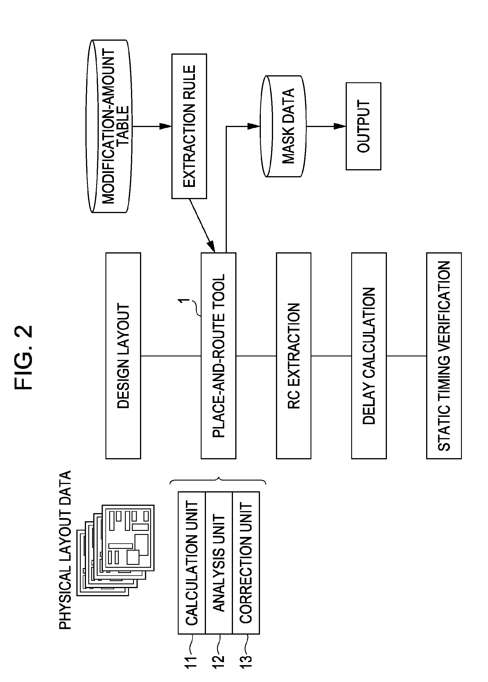
[0059]FIG. 2 is a flowchart illustrating a mask data generation process according to a first embodiment of the present invention.
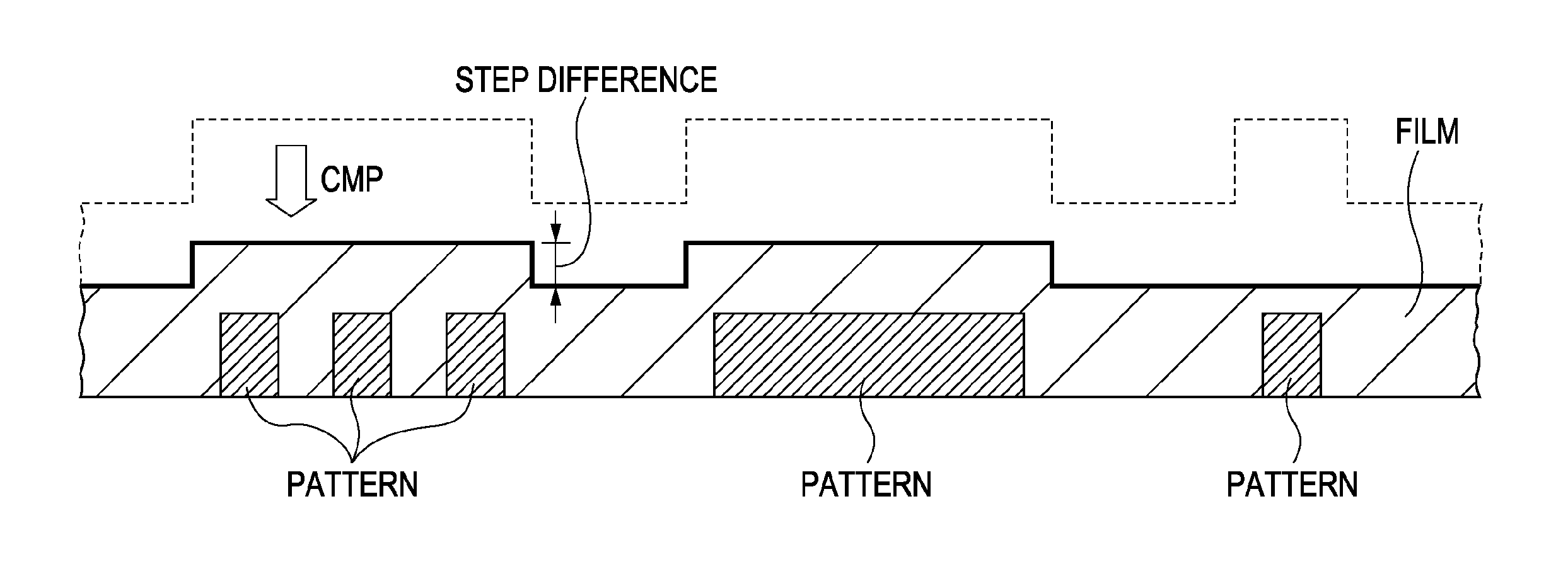
[0060]First, the design layout data (physical layout data) of a circuit to be manufactured is input to a place-and-route tool 1. Additionally, a modification amount table in which the preset amounts of modifications of pattern widths, and extraction rules regarding the coverage ratio of the pattern are input to the place-and-route tool 1. Here, the coverage ratio refers to the percentage of the area in plan view of a pattern in the area in plan view of the physical layout.
[0061]Next, the calculation unit 11 in the place-and-route tool 1 performs a process for resizing (modifying) the pattern width from the input design layout data in accordance with a modification amount table. The modification amount table is a table in which the amounts of modifications are set in accordance with the type of film formed on a pattern. The calculation unit 11 resizes the p...
second embodiment
[0089]A second embodiment is directed to an example in which a type of film whose shape of a formed film described in the first embodiment differs is used, an extraction algorithm is changed to extract a critical step-difference portion, and a semiconductor device is manufactured. Therefore, the basic flow of the manufacture is the same as that of the first embodiment, and the extraction algorithm differs. FIG. 6 illustrates an algorithm for extracting a critical step-difference pattern in the second embodiment. This algorithm is an algorithm for extracting a critical step-difference pattern with regard to a pattern having a high coverage ratio and a large area, which is an algorithm (1) shown in FIG. 3.
[0090]First, resizing of −30% to −50% of the amount of film formation is performed on a layout pattern. After that, the coverage ratio of the layout in the pattern after resizing is calculated. At this time, the layout is divided into mesh elements of 50 μm, and a calculation is made...
PUM
 Abstract
Description
Claims
Application Information