Thin film transistors and arrays

a thin film transistor and array technology, applied in the field of thin film transistors, can solve the problems of difficult control of threshold voltage, and achieve the effect of reducing the magnitude of threshold voltage and the off-state leakage current of

Active Publication Date: 2010-12-02
SHIH ISHIANG +3
View PDF3 Cites 38 Cited by
  • Summary
  • Abstract
  • Description
  • Claims
  • Application Information

AI Technical Summary

Benefits of technology

[0014]Still another object of this invention is to provide thin film transistor structures having a passivation layer with fixed charges, which are negative for n-channel TFTs and positive for p-channel...

Problems solved by technology

However, for TFTs with high mobility active channels, the values of IOFF are often more sensitive to processing conditions and can be quite large even with a s...

Method used


Image

  • Thin film transistors and arrays
  • Thin film transistors and arrays
  • Thin film transistors and arrays

Examples


Embodiment Construction

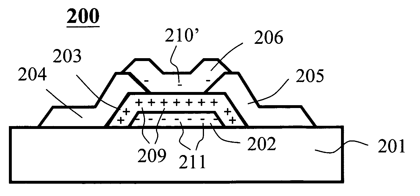
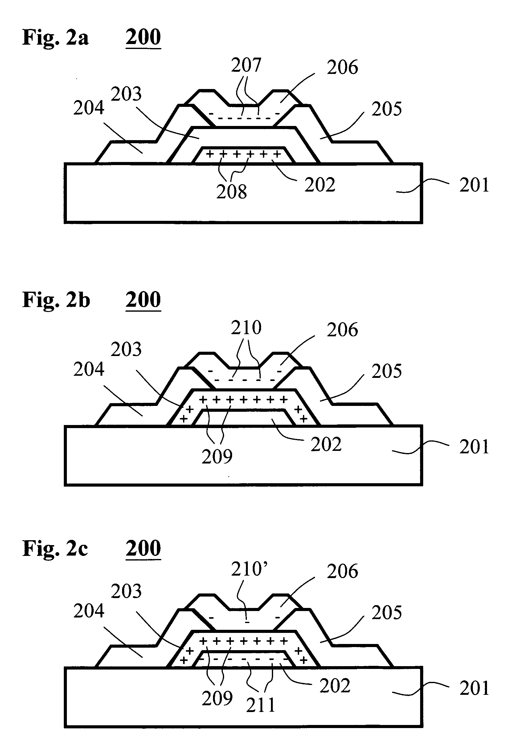
[0026]In order to simplify the following descriptions, only n-channel TFT structures with controllable threshold voltage and reduced OFF state current are presented. However, it should be apparent to anyone of skill in the art that p-channel TFT structures with controllable threshold voltage and reduced OFF state current can be obtained by changing sign of the fixed charges in the gate insulators and the passivation layer. Furthermore, TFTs of top gate structure with controllable threshold voltage and reduced OFF state current can be easily obtained by modify the bottom gate structures presented below.

[1] Normal Double Gate Insulators:

[0027]A preferred embodiment of this invention is illustrated in FIG. 5 where a cross section of a n-channel TFT (500) is shown to have a first substrate (501), a first gate electrode (502), a first gate insulator (503) having a first fixed charges (504), a second gate insulator (505) having a second fixed charges (506), a source (507) with projection ...


PUM


Abstract

Thin film transistors and arrays having controlled threshold voltage and improved ION/IOFF ratio are provided in this invention. In one embodiment, a thin film transistor having a first gate insulator of high breakdown field with positive fixed charges and a second gate insulator with negative fixed charges is provided; said negative fixed charges substantially compensate said positive fixed charges in order to reduce threshold voltage and OFF state threshold voltage of said transistor. In another embodiment, a thin film transistor having a first passivation layer with negative fixed charges is provided, the negative charges reduce substantially unwanted negative charges in the adjacent active channel and hence reduce the OFF state current and increase ION/IOFF ratio, which in turn reduce the threshold voltage of the transistor.

Description

FIELD OF THE INVENTION[0001]This invention is related to thin film transistors for electronic and optoelectronic applications. More specifically, it relates to thin film transistors with controllable threshold voltages and reduced OFF state currents.BACKGROUND ON THE INVENTIONThin Film Transistor Technology[0002]In large area electronic circuits such as active-matrix liquid crystal display (AM-LCD) technology, active-matrix organic light emitting displays (AM-OLED) and x-ray imagers, thin film transistors (TFTs) are used to form the switching circuits. At least one thin film transistor is required to form into a pixel of the circuits.[0003]A schematic diagram of a pixel (100) in typical AM-LCD technology is shown in FIG. 1. A TFT (101) is deposited on a first substrate (110). During operation, the TFT (101) behaves like a variable resistor with low RON in ON state and high ROFF in OFF state. The ON and OFF states of TFT are controlled by the voltage supplied from the gate select lin...

Claims


Application Information

Patent Timeline
IPC IPC(8): H01L27/088H01L29/786
CPCH01L29/78609H01L29/4908
Inventor SHIH, ISHIANGQIU, CINDY X.QIU, CHUNONGSHIH, YI-CHI
Owner SHIH ISHIANG
Why Eureka
Try Eureka