Semiconductor light emitting element

Active Publication Date: 2010-12-02
SHIN-ETSU HANDOTAI CO LTD
View PDF10 Cites 19 Cited by
  • Summary
  • Abstract
  • Description
  • Claims
  • Application Information

AI Technical Summary

Benefits of technology

[0012]Therefore, it is an object of the invention to provide a semiconductor lig

Problems solved by technology

However, the light extraction efficiency of the light emitting element is still low, so that it is more important to improve the light extraction efficiency.
However, since the bandgap of the GaAs substrate is narrower than that of the light emitting layer, most of light emitted from the light emitting layer is absorbed by the GaAs substrate such that the light ex

Method used


Image

  • Semiconductor light emitting element
  • Semiconductor light emitting element
  • Semiconductor light emitting element

Examples


example 1

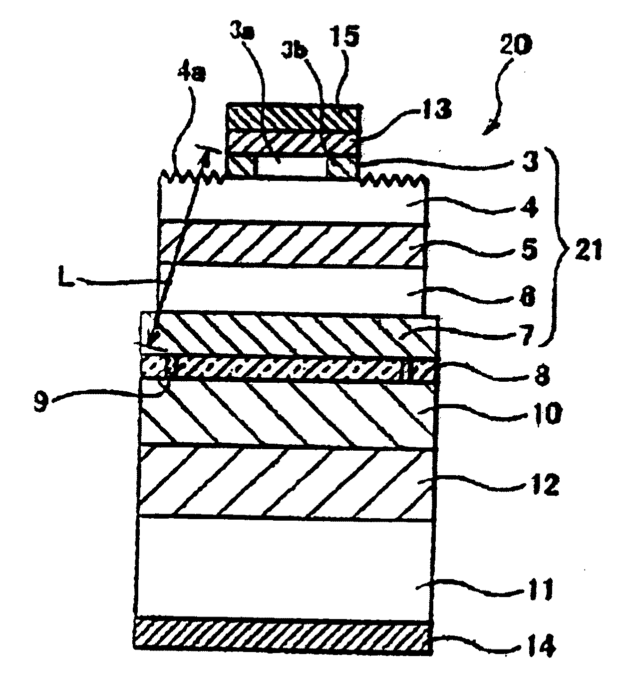
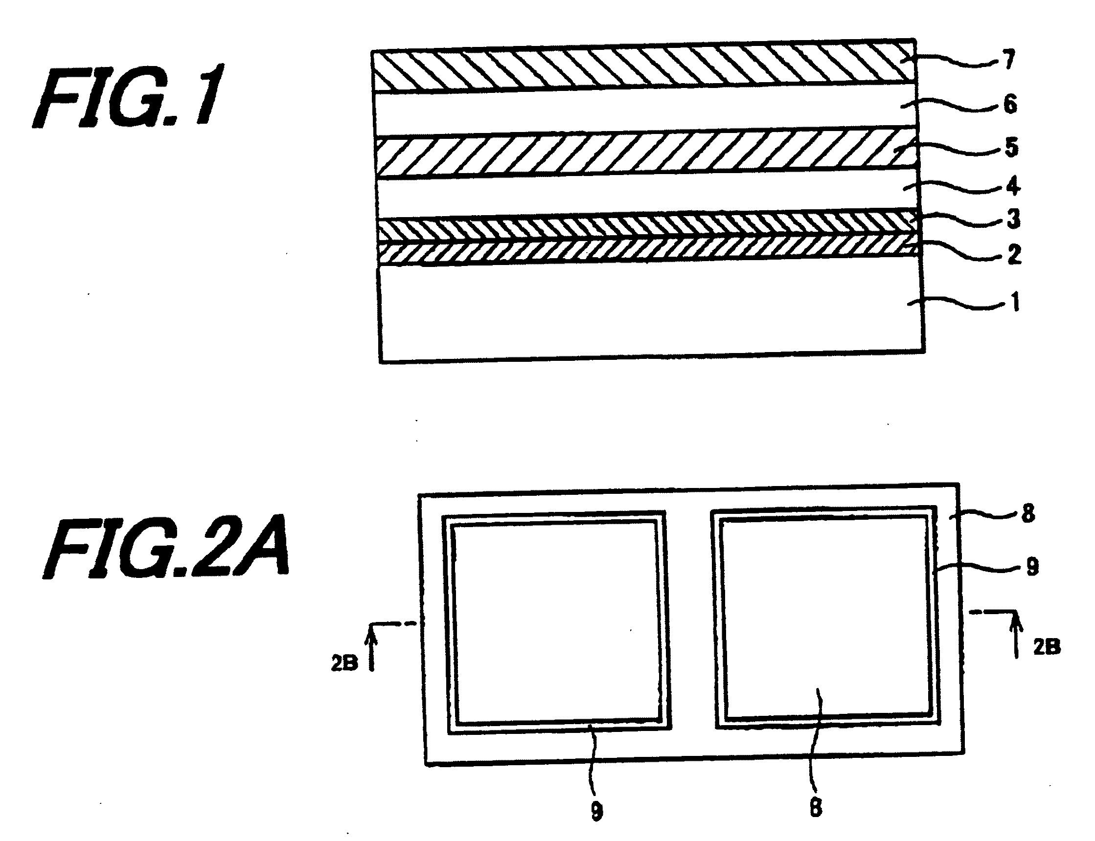
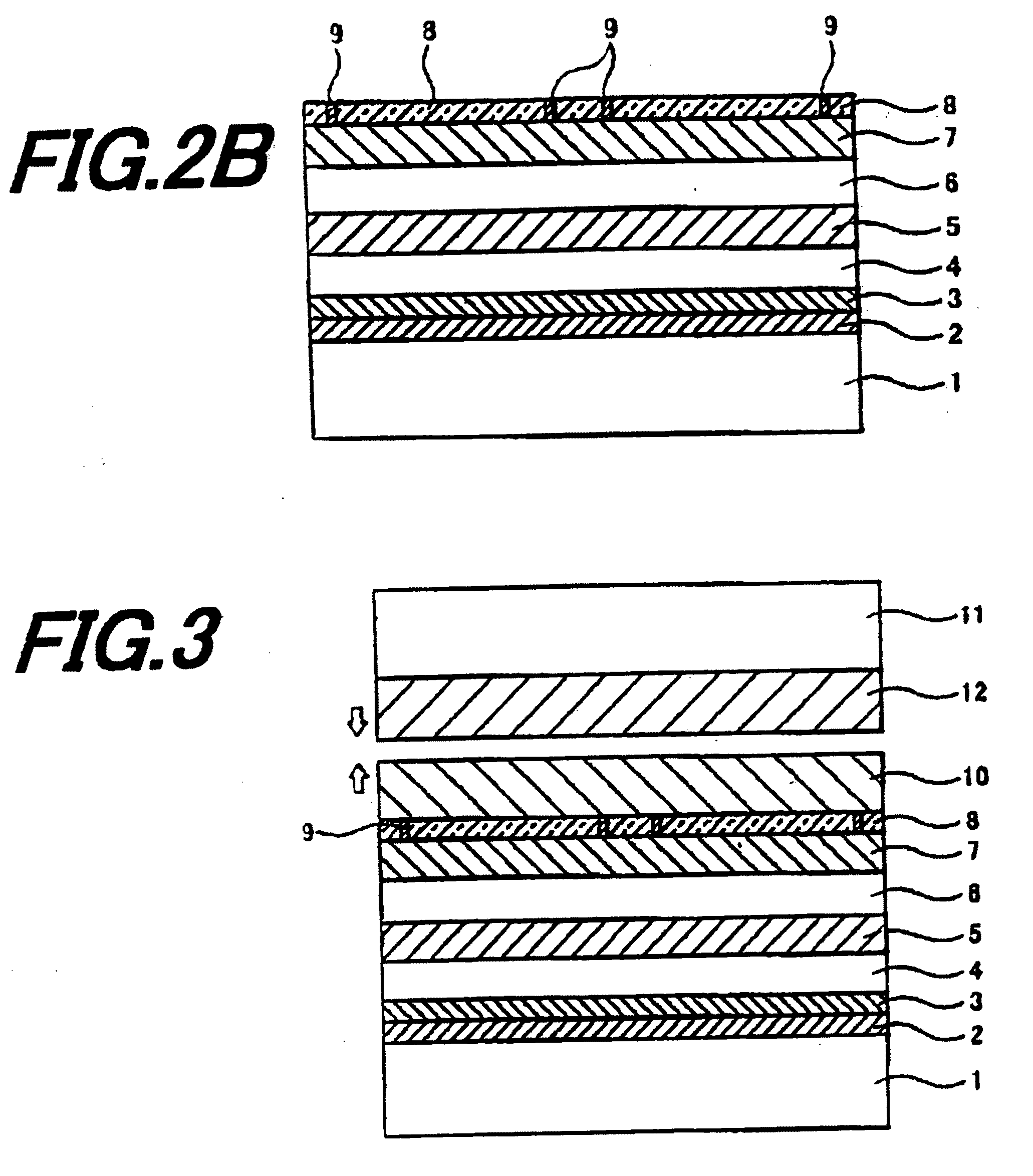
[0082]FIGS. 7A and 7B schematically show a semiconductor light emitting element of Example 1 according to the invention. FIGS. 1 to 6 are cross-sectional views schematically showing each process of a method of manufacturing a semiconductor light emitting element according to Example 1 of the invention. Further, in order to simplify the drawings, FIGS. 1 to 6 show situations that two light emitting elements 20 are manufactured in the condition of being arranged side by side.

[0083]First, an epitaxial wafer for a red LED having a structure shown in FIG. 1 and having a light emitting wavelength at or near 630 nm was manufactured. An epitaxial growth method, an epitaxial structure, a electrode forming method and an LED element manufacturing method are as follows.

[0084]In the epitaxial growth, an undoped (Al0.7G4.3)0.5In0.5P etching stop layer 2, an n-type (Si-doped) GaAs contact layer 3, an n-type (Si-doped) (Al0.7Ga0.3)0.5In0.5P clad layer 4, an undoped (Al0.1Ga0.9)0.5In0.5P active laye...


PUM


Abstract

A semiconductor light emitting element includes a group III-V compound semiconductor layer, a first main surface and a second main surface, a reflection metal film formed on the second main surface, a front surface electrode formed on the first main surface, and an ohmic contact joint part formed between the reflection metal film and the group III-V compound semiconductor layer except a region directly under the front surface electrode. The ohmic contact joint part is disposed in a side of an outer peripheral part of the semiconductor light emitting element, formed so as to surround the front surface electrode when the ohmic contact joint part is viewed from a side of the front surface electrode, and disposed so that distance from each location of outer edge parts of the front surface electrode to the ohmic contact joint part nearest to the each location becomes equal to each other.

Description

[0001]The present application is based on Japanese patent application No. 2009-127434 filed on May 27, 2009, the entire contents of which are incorporated herein by reference.BACKGROUND OF THE INVENTION[0002]1. Field of the Invention[0003]This invention relates to a semiconductor light emitting element that is structured such that an ohmic contact joint part and a reflection metal film are sandwiched between a group III-V compound semiconductor layer including a light emitting layer and a support substrate. In particular, this invention relates to a semiconductor light emitting element with improved light extraction efficiency.[0004]2. Description of the Related Art[0005]Recently, for light emitting diodes (LEDs) as a semiconductor light emitting element, GaN or AlGaInP-based high quality crystals can be grown by metal-organic vapor phase epitaxy (MOVPE), so as to produce high brightness blue, green, orange, yellow and red LEDs. Along with the development of the high brightness LEDs...

Claims


Application Information

Patent Timeline
IPC IPC(8): H01L33/46
CPCH01L33/0079H01L33/22H01L33/42H01L33/405H01L33/387H01L33/0093
Inventor IIZUKA, KAZUYUKIWATANABE, MASAHIRO
Owner SHIN-ETSU HANDOTAI CO LTD
Why Eureka
Try Eureka