Plasma processing apparatus and plasma processing method

a plasma processing apparatus and plasma technology, applied in the direction of electrical apparatus, basic electric elements, electric discharge tubes, etc., can solve the problems of plasma sheath deformation, potential difference between substrate (mounting table) and focus ring during plasma process, and protruding substrate, etc., to reduce deposits, reduce deposits, and reduce deposits

Active Publication Date: 2010-12-02
TOKYO ELECTRON LTD
View PDF4 Cites 33 Cited by
  • Summary
  • Abstract
  • Description
  • Claims
  • Application Information

AI Technical Summary

Benefits of technology

[0014]In view of the foregoing, the present disclosure provides a plasma processing apparatus capable of effectively finding an optimum voltage to be applied to a conductive ring in order to reduce deposits on a peripheral portion of a substrate as well as improve a process result in balance and capable of accurately and simply adjusting the optimum application voltage without changing a shape (e.g., height of a top surface) of a focus ring.
[0015]The present inventor has studied a method of effectively finding an optimum application voltage in order to increase both the effect of reducing deposits on a peripheral portion of a substrate and the effect of improving a process result (e.g., improving inclination of an etching profile) without changing a shape (e.g., height of a top surface) of a focus ring. As a result of the study, it has been found that when a focus ring is configured such that a conductive ring is installed in a floating state on a dielectric ring provided on a mounting table, if plasma is generated, a floating voltage is generated at the conductive ring. In this case, an application voltage can be determined to be in the range from an electric potential of the conductive ring by the floating voltage to an electric potential of the plasma. Therefore, it is possible to effectively find the optimum application voltage for reducing the deposits on the peripheral portion of the substrate as well as improving the process result in balance.

Problems solved by technology

Generally, in such a plasma processing apparatus, there has been a problem in that the peripheral portion of the substrate is protruded from the mounting table and there is a gap between the mounting table and the focus ring.
However, as disclosed in Patent Document 2, for example, when the mounting table and the focus ring are insulated from each other via the dielectric member provided therebetween, a potential difference between the substrate (mounting table) and the focus ring is generated during a plasma process.
However, even if the optimum focus ring is found, the focus ring may be eroded through repeated plasma etching processes and, thus, its height may be changed and the plasma sheath may be deformed again.
However, since the incident angle of the ions in the plasma entered into the gap between the substrate and the focus ring becomes also nearly vertical, it becomes difficult for the ions to reach, e.g., a rear surface of the peripheral portion of the substrate.
Therefore, it is difficult to improve these both effects in balance only by adjusting the height of the top surface of the focus ring.
Therefore, process or configuration becomes complicated to find such an optimum voltage or its adjustment voltage.
Accordingly, it is impossible to improve the effect of reducing the deposits on the peripheral portion of the substrate.
However, there is no description of a method of finding an optimum application voltage.
Therefore, in case of finding the optimum voltage according to a conventional way as described in Patent Document 1, a process or configuration becomes complicated, and, thus, much time and effort are required.

Method used


Image

  • Plasma processing apparatus and plasma processing method
  • Plasma processing apparatus and plasma processing method
  • Plasma processing apparatus and plasma processing method

Examples


Embodiment Construction

[0046]Hereinafter, embodiments of the present disclosure will be described in detail with reference to the accompanying drawings. In this specification and drawings, same parts having substantially the same function and configuration will be assigned same reference numerals, and redundant explanation thereof will be omitted.

[0047](Configuration Example of Plasma Processing Apparatus)

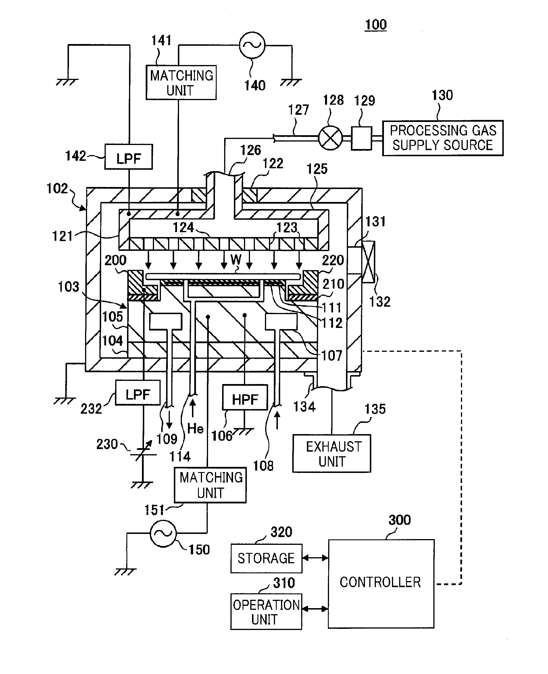
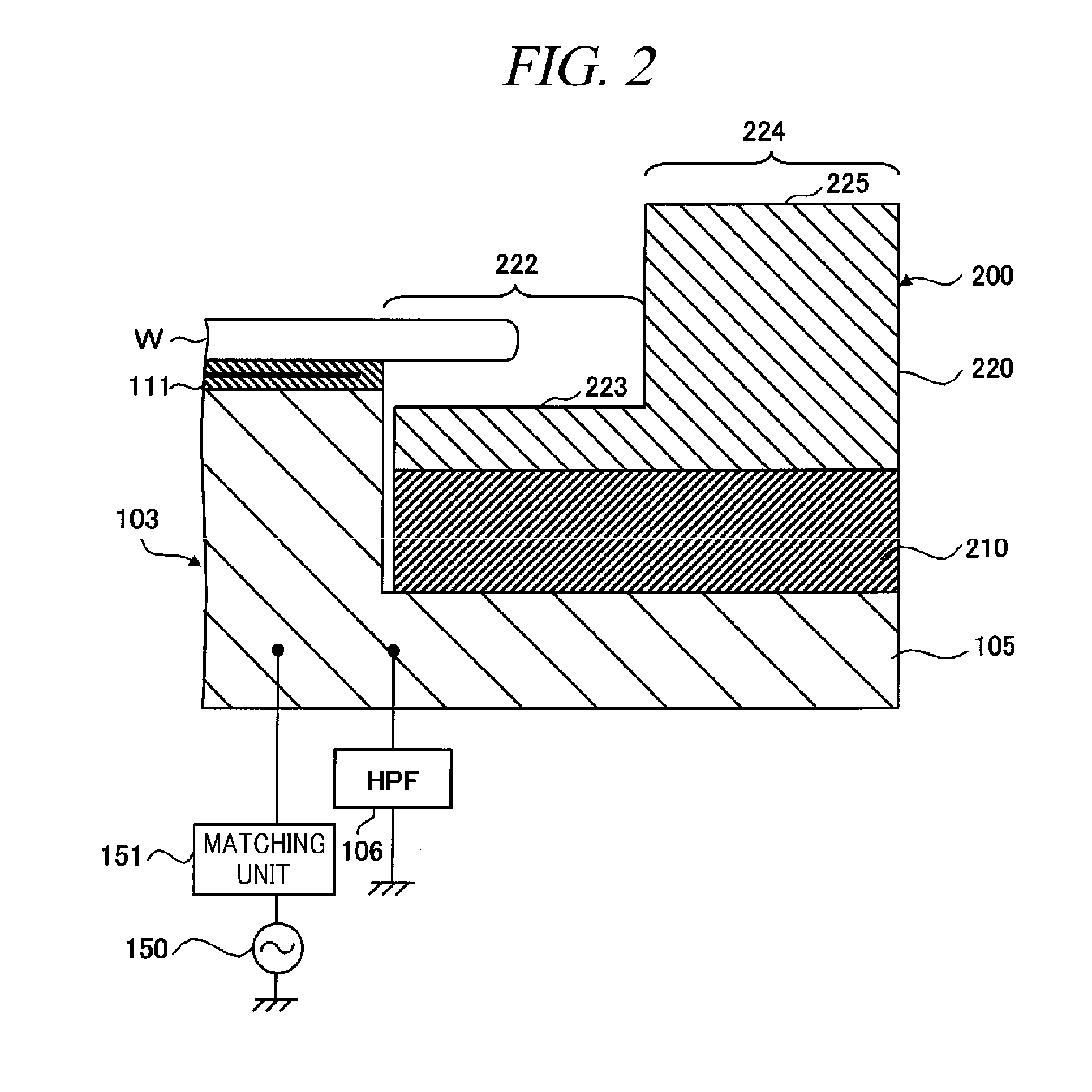
[0048]First, there will be explained a schematic configuration of a plasma processing apparatus in accordance with an embodiment of the present disclosure with reference to the accompanying drawings. FIG. 1 is a cross sectional view of a schematic configuration of the plasma processing apparatus in accordance with the present embodiment. Hereinafter, as one example of the plasma processing apparatus, a parallel plate type plasma etching apparatus will be described.

[0049]For example, a plasma processing apparatus 100 includes a processing chamber 102 having a cylindrical processing vessel made of aluminum...


PUM

PropertyMeasurementUnit
DC voltageaaaaaaaaaa
frequencyaaaaaaaaaa
frequencyaaaaaaaaaa

Abstract

An optimum application voltage for reducing deposits on a peripheral portion of a substrate as well as improving a process result in balance is effectively found without changing a height of a focus ring. A plasma processing apparatus includes a focus ring which includes a dielectric ring provided so as to surround a substrate mounting portion of a mounting table and a conductive ring provided on the dielectric ring; a voltage sensor configured to detect a floating voltage of the conductive ring; a DC power supply configured to apply a DC voltage to the conductive ring. An optimum voltage to be applied to the conductive ring is obtained based on a floating voltage actually detected from the conductive ring, and the optimum application voltage is adjusted based on a variation in the actually detected floating voltage for each plasma process.

Description

CROSS-REFERENCE TO RELATED APPLICATION[0001]This application claims the benefit of Japanese Patent Application No. 2009-133269 filed on Jun. 2, 2009, and U.S. Provisional Application Ser. No. 61 / 222,798 filed on Jul. 2, 2009, the entire disclosures of which are incorporated herein by reference.FIELD OF THE INVENTION[0002]The present disclosure relates to a plasma processing apparatus including a mounting table for mounting thereon a substrate and a focus ring installed on the mounting table so as to surround the substrate, a plasma processing method, and a program.BACKGROUND OF THE INVENTION[0003]In manufacturing a semiconductor device, a plasma etching process is repeatedly performed on a substrate such as a semiconductor wafer, a FPD substrate, or a substrate for a solar cell so as to form a micro circuit pattern thereon. In the plasma etching process, for example, plasma is generated by applying a high frequency voltage to electrodes placed to face each other within a depressuriz...

Claims


Application Information

Patent Timeline
Patent Type & Authority Applications(United States)
IPC IPC(8): H01L21/3065C23F1/08H01L21/306
CPCH01J37/32091H01J37/32623H01J37/32642H01L21/205H01L21/302H01L21/3065H01L21/76825H01L21/76826
Inventor KOSHIMIZU, CHISHIO
Owner TOKYO ELECTRON LTD
Why Eureka
Try Eureka