Insulated gate bipolar transistor (IGBT) with monolithic deep body clamp diode to prevent latch-up

a technology of deep body clamp diode, which is applied in the direction of basic electric elements, electrical apparatus, semiconductor devices, etc., can solve the problems of slow switching speed, adverse effect on the switching speed of igbt devices, and the difficulty of preventing latching up of conventional high-voltage semiconductor power devices such as insulated gate bipolar transistors (igbts) devices, so as to improve the switching speed and prevent latching

Active Publication Date: 2010-12-09
FORCE MOS TECH CO LTD
View PDF3 Cites 25 Cited by
  • Summary
  • Abstract
  • Description
  • Claims
  • Application Information

AI Technical Summary

Benefits of technology

[0009]It is therefore an aspect of the present invention to provide a new and improved insulation gate bipolar transistor (IGBT) power device by forming deep-body dopant regions in the emitter-base contact regions to form deep-body cla

Problems solved by technology

Conventional device configuration and manufacturing methods for providing the insulated gate bipolar transistor (IGBT) devices are often confronted with two technical difficulties. FIG. 1 illustrates the first technical difficulties of latch-up due to the intrinsic parasitic thyristor formed as NPN and PNP transistors formed in parallel across the collector and emitter.
The second technical difficulty is the slow switching speed due to operations of current conduction that involves two electric carriers, i.e., injection of electrons from the N+ emitter and holes from the P+ emitter.
The switching speed of the IGBT devices is adversely affected due to these extra charged car

Method used


Image

  • Insulated gate bipolar transistor (IGBT) with monolithic deep body clamp diode to prevent latch-up
  • Insulated gate bipolar transistor (IGBT) with monolithic deep body clamp diode to prevent latch-up
  • Insulated gate bipolar transistor (IGBT) with monolithic deep body clamp diode to prevent latch-up

Examples


Embodiment Construction

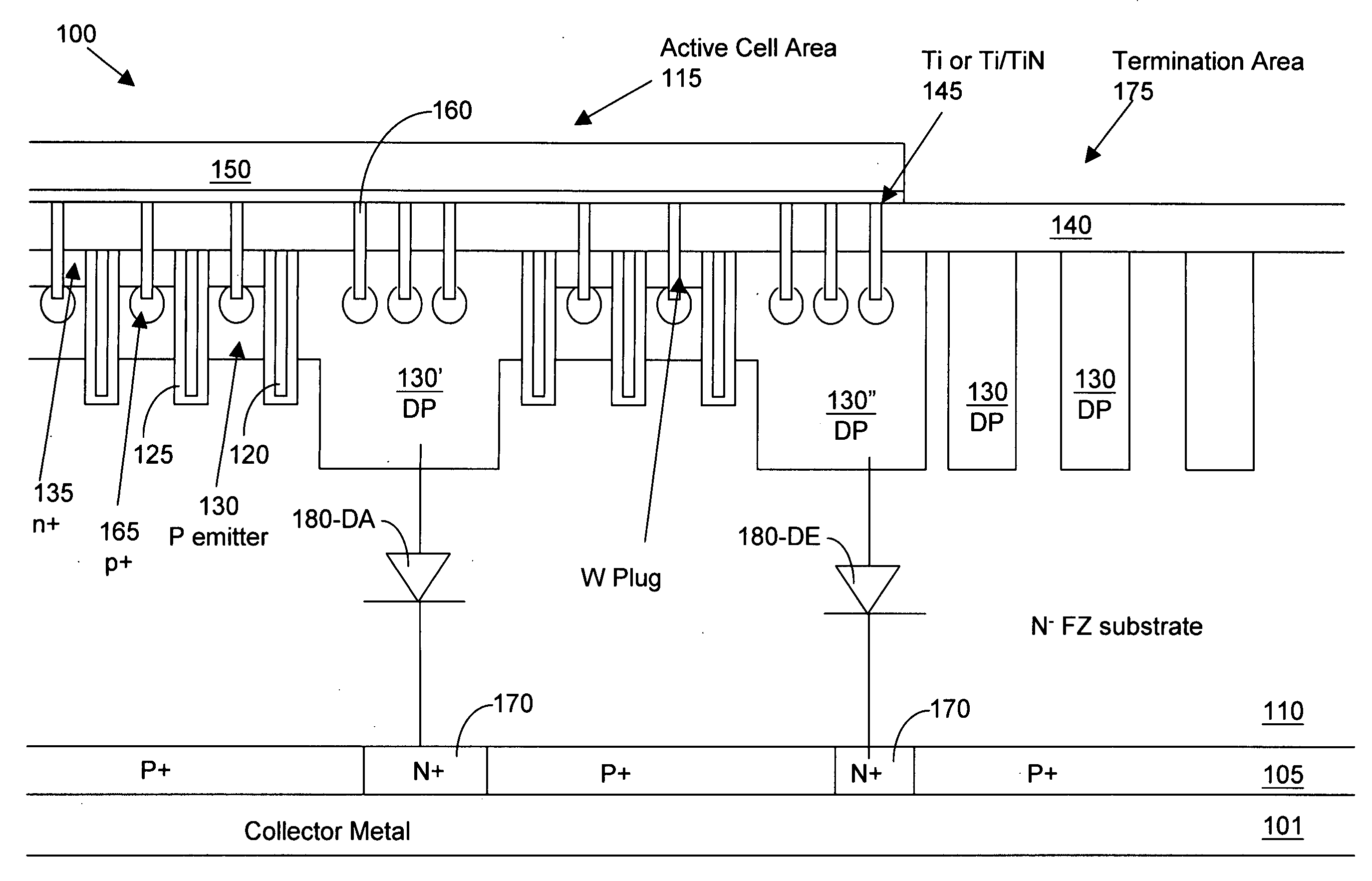
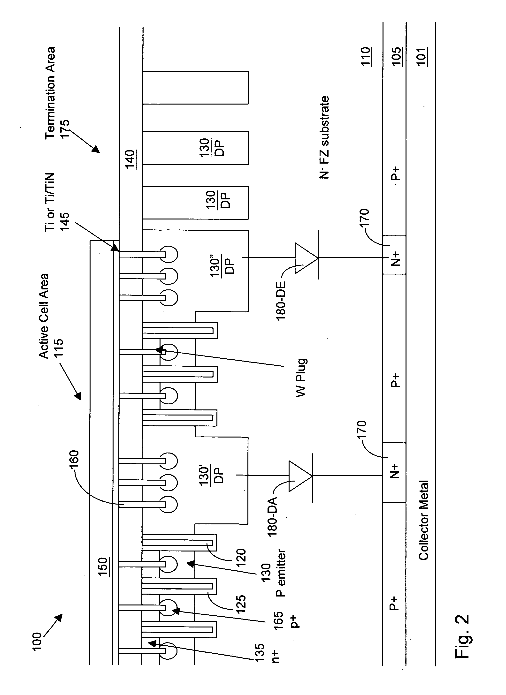
[0017]Referring to FIG. 2 for a side cross sectional view of an insulated gate bipolar transistor (IGBT) device 100 formed as a vertical power device on a N-semiconductor substrate 110 functioning as an N-base layer. The P+ regions 105 formed at the bottom surface of the substrate 110 function as a collector region with a collector metal 101 formed on the bottom surface. The P+ collector regions further includes N+ dopant regions 170 formed under the deep body regions 130′ for connection to a diode 180-DA and 180-DE as will be described below. The P+ collector regions 105 are formed on rear side of the N− substrate 110. The IGBT device further comprises trench gates 120 filled with gate dielectric layer such as polysilicon and padded with gate oxide layer 125. The trench gates are surrounded by P-base regions 130 that encompass N+ emitter regions 135 formed near the top surface of the substrate. The top surface of the substrate is covered with an insulation layer 140 on overlaying a...


PUM


Abstract

A trench insulation gate bipolar transistor (IGBT) power device with a monolithic deep body clamp diode comprising a plurality of trench gates surrounded by emitter regions of a first conductivity type near a top surface of a semiconductor substrate of the first conductivity type encompassed in base regions of a second conductivity type. The trench semiconductor power device further comprises a collector region of the second conductivity type disposed on a rear side opposite from the top surface of the semiconductor substrate corresponding to and underneath the trench gates surrounded by the emitter regions encompassed in the base regions constituting a plurality of insulation gate bipolar transistors (IGBTs). The IGBT power device further includes a deep dopant region of the second conductivity type having P-N junction depth deeper than the base region, disposed between and extending below the trench gates in the base region of the first conductivity type. The IGBT power device further includes a dopant region of the first conductivity type disposed on the rear side of the semiconductor substrate corresponding to and underneath the deep dopant region disposed between the trench gates thus constituting a plurality of deep body diodes.

Description

BACKGROUND OF THE INVENTION[0001]1. Field of the Invention[0002]The invention relates generally to a device configuration and method of manufacturing an insulated gate bipolar transistor (IGBT). More particularly, this invention relates to an improved IGBT device configuration and manufacturing method for a trench IGBT that has a monolithic deep body clamp diode for preventing latch-up, and allowing reverse current to flow through the diode when the IGBT is turned off in many power switching applications such as inverter and H-Bridge motor switching circuits.[0003]2. Description of the Relevant Art[0004]Conventional device configuration and manufacturing methods for providing the insulated gate bipolar transistor (IGBT) devices are often confronted with two technical difficulties. FIG. 1 illustrates the first technical difficulties of latch-up due to the intrinsic parasitic thyristor formed as NPN and PNP transistors formed in parallel across the collector and emitter. The second te...

Claims


Application Information

Patent Timeline
IPC IPC(8): H01L29/739
CPCH01L29/0619H01L29/0696H01L29/861H01L29/7397H01L29/456H01L29/0834
Inventor HSHIEH, FWU-IUAN
Owner FORCE MOS TECH CO LTD
Why Eureka
Try Eureka