Programmable gain MOS amplifier

a mos amplifier and programmable gain technology, applied in the direction of amplifiers with field-effect devices, gain control, gated amplifiers, etc., can solve the problem of complicated linear adjustment of gain in db

Active Publication Date: 2010-12-09
MEDIATEK INC
View PDF8 Cites 12 Cited by
  • Summary
  • Abstract
  • Description
  • Claims
  • Application Information

AI Technical Summary

Benefits of technology

[0007]The present invention provides a programmable gain MOS amplifier for outputting an amplified signal at a first end of a load with a programmable gain. The programmable gain MOS amplifier comprises a first gain provider for providing a first predetermined gain, comprising a MOS transistor having a first predetermined aspect ratio corresponding to the first predetermined gain, the MOS transistor comprising a control end coupled to an input end of the programmable gain MOS amplifier for receiving an input signal; a biasing end coupled to a biasing source; and an output end; and a first gain tuner for adjusting the first predetermined gain, comprising a gain enabling module, comprising a MOS transistor, comprising a control end for receiving a first controlling signal; a first end coupled to the first end of the load; and a second end coupled to the output end of the MOS transistor of the first gain provider; and a gain decreasing module, comprising a first MOS transistor, comprising a control end for receiving a second controlling signal; a first end coupled to a second end of the load; and a second end coupled to the output end of the MOS transistor of the first gain provider; wherein when the first controlling signal turns on the MOS transistor of the gain enabling module of the first gain tuner, the programmable gain equals the G1; when the first controlling signal turns on the MOS transistor of the gain enabling module of the first gain tuner and the second controlling signal turns on the first MOS transistor of the gain decreasing module of the first gain tuner, the programmable gain equals [M1 / (M1+M2)]×G1; M1 represents an aspect ratio of the MOS transistor of the gain enabling module of the first gain tuner, M2 represents an aspect ratio of the first MOS transistor of the gain decreasing module of the first gain tuner, and G1 represents the first predetermined gain.
[0008]The present invention further provides a programmable gain MOS amplifier for outputting an amplified signal at a first end of a load with a programmable gain according to a gain level data. The programmable gain MOS amplifier comprises a decoder for decoding the gain level data to a plurality of controlling signals; a plurality of gain providers, each gain provider providing a predetermined gain, each gain provider comprising a MOS transistor having a predetermined aspect ratio corresponding to a corresponding predetermined gain, the MOS transistor comprising a control end coupled to an input end of the programmable gain MOS amplifier for receiving an input signal; a biasing end coupled to a biasing source; and an output end; and a plurality of gain tuners, each gain tuner adjusting a predetermined gain from corresponding one of the plurality of the gain providers, each gain tuner comprising a gain enabling module, comprising a MOS transistor, comprising a control end, coupled to the decoder, for receiving a corresponding controlling signal; a first end coupled to the first end of the load; and a second end coupled to the output end of the MOS transistor of the corresponding gain provider; wherein a predetermined gain provided from one of the plurality of the gain providers is added to the programmable gain of the MOS amplifier when the MOS transistor of the gain enabling module of the corresponding gain tuner is turned on by the corresponding controlling signal decoded from the gain level data.
[0009]The present invention further provides a programmable gain MOS amplifier for outputting an amplified signal at a first end of a load with a programmable gain according to a gain level data. The programmable gain MOS amplifier comprises a decoder for decoding the gain level data to a plurality of controlling signals; a first gain provider for providing a first predetermined gain, comprising a first MOS transistor having a first predetermined aspect ratio corresponding to the first predetermined gain, the first MOS transistor comprising a control end coupled to an input end of the programmable gain MOS amplifier for receiving an input signal; a biasing end coupled to a biasing source; and an output end; and a first gain tuner for adjusting the first predetermined gain, comprising a gain enabling module, comprising a second MOS transistor, comprising a control end coupled to the decoder for receiving a corresponding controlling signal; a first end coupled to the first end of the load; and a second end coupled to the output end of the second MOS transistor of the first gain provider; and a gain decreasing module, comprising M third MOS transistors, each third MOS transistor comprising a control end coupled to the decoder for receiving a corresponding controlling signal; a first end coupled to a second end of the load; and a second end coupled to the output end of the corresponding third MOS transistor of the first gain provider; a second gain provider for providing a second predetermined gain, comprising a fourth MOS transistor having a second predetermined aspect ratio corresponding to the second predetermined gain, the fourth MOS transistor comprising a control end coupled to the input end of the programmable gain MOS amplifier for receiving the input signal; a biasing end coupled to the biasing source; and an output end; and a second gain tuner for adjusting the second predetermined gain, comprising a gain enabling module, comprising a fifth MOS transistor, comprising a control end coupled to the decoder for receiving a corresponding controlling signal; a first end coupled to the first end of the load; and a second end coupled to the output end of the fifth MOS transistor of the second gain provider; wherein the second predetermined gain is higher than the first predetermined gain; wherein the programmable gain is obtained from the first predetermined gain adjusted by the first gain tuner and the second predetermined gain adjusted by the second gain tuner.

Problems solved by technology

However, since the exponential characteristic does not exist between the gate-source voltage (VGS) of a MOS and its corresponding output current ID, it is complicated to achieve adjusting the gain in dB linearly by linearly adjusting the magnitude of the controlling signal with a MOS amplifier.

Method used


Image

  • Programmable gain MOS amplifier
  • Programmable gain MOS amplifier
  • Programmable gain MOS amplifier

Examples


first embodiment

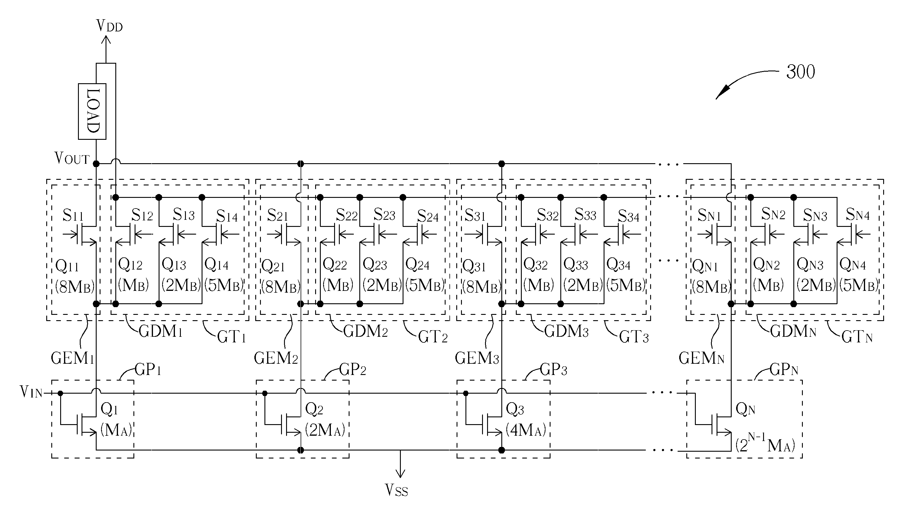
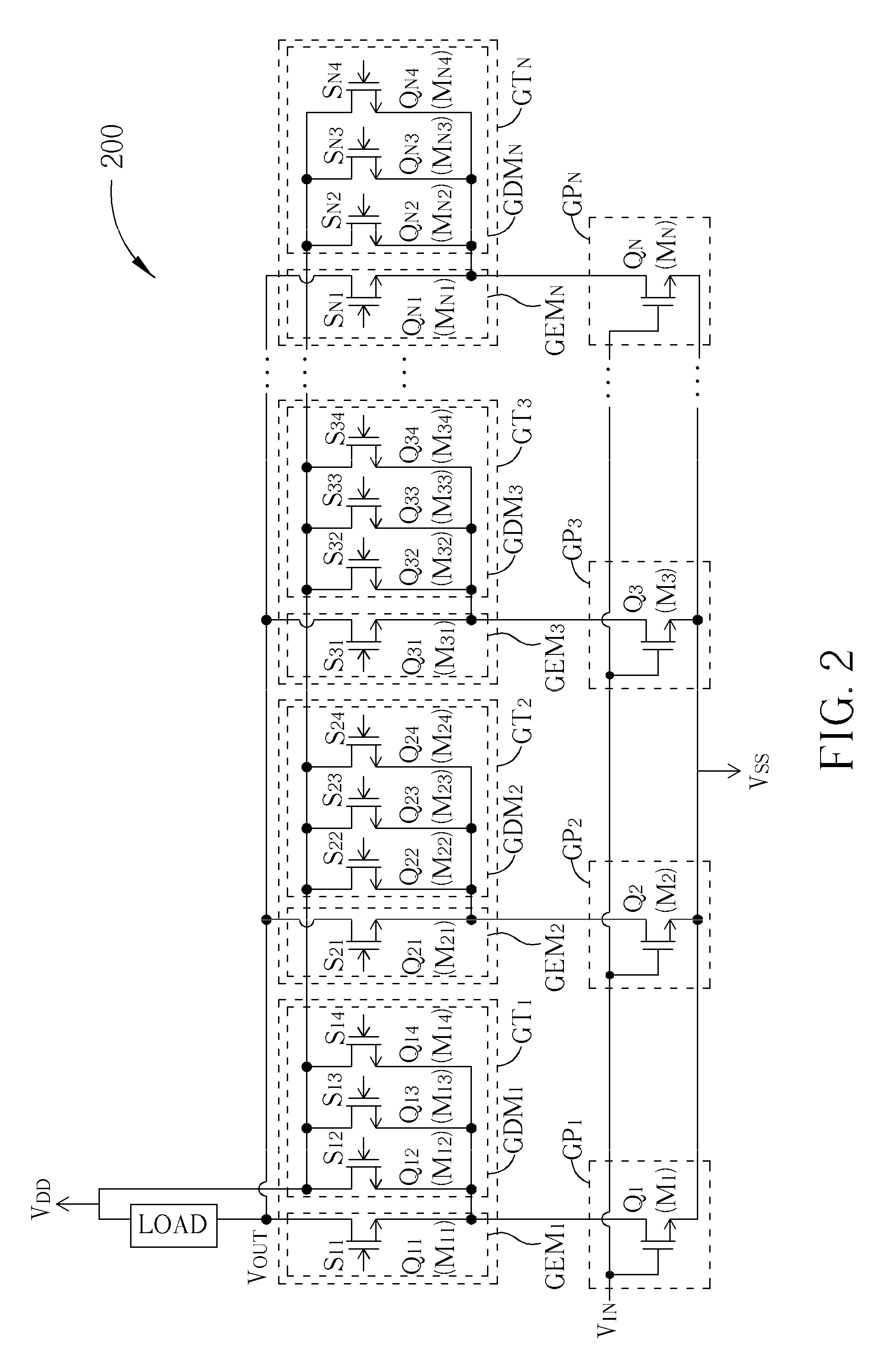
[0019]Please refer to FIG. 2. FIG. 2 is a diagram illustrating a MOS amplifier 200 according to the present invention. As shown in FIG. 2, the MOS amplifier 200 comprises N gain providers GP1˜GPN, and N gain tuners GT1˜GTN.

[0020]Each gain tuner further comprises a gain enabling module GEM and a gain decreasing module GDM. For example, the gain tuner GT1 comprises the gain enabling module GEM1 and the gain decreasing module GDM1. Each gain enabling module GEM is realized with a MOS transistor. For example, the gain enabling module GEM1 is realized with the MOS transistor Q11 having an aspect ratio M11. Each gain decreasing module GDM is realized with three MOS transistors. For example, the gain decreasing module GDM1 is realized with the MOS transistors Q12, Q13, and Q14 having aspect ratio M12, M13, and M14, respectively. Each gain tuner corresponds to a gain provider. For example, the gain tuner GT1 corresponds to the gain provider GP1. Additionally, the sum of the aspect ratios of...

second embodiment

[0032]Please refer to FIG. 4. FIG. 4 is a diagram illustrating a MOS amplifier 400 according to the present invention. As shown in FIG. 4, the MOS amplifier 400 comprises two gain providers GP1 and GP2, two gain tuners GT1 and GT2, N gain providers GPT1˜GPTN, and N gain tuners GTTI˜GTTN.

[0033]The functional description for the gain providers, the gain tuners in FIG. 4 is similar to those components in FIG. 2 and is omitted. However, structurally, MOS amplifier 400 is slightly changed according to the MOS amplifier 200. As shown in FIG. 4, only two gain providers GP1 and GP2 and their corresponding gain tuners GT1 and GT2 are utilized for low gain adjustment range, but N gain provider GPT1˜GPTN and their corresponding gain tuners GTT1˜GTTN are utilized for high gain adjustment range. More particularly, the aspect ratios of the MOS transistors Q1 and Q2 respectively of the gain providers GP1 and GP2 can be designed to be M1 and 2M1 and the aspect ratio of the MOS transistor QT1 of the...

third embodiment

[0036]Please refer to FIG. 5. FIG. 5 is a diagram illustrating a MOS amplifier 500 according to the present invention. The MOS amplifier 500 is disclosed as a design example for 36 dB gain adjustment range. As shown in FIG. 5, the MOS amplifier 500 comprises the gain providers GP5, GP6, GP7, GP8, GP9, and GP10, and the gain tuners GT5, GT6, GT7, GT8, GT9, and GT10. It is noticeable that each of the gain tuners GT5, GT8, GT9, and GT10 only comprises the gain enabling module, and the corresponding gain decreasing module is saved. It is noticeable that the embodiment as shown in FIG. 5 is designed as the above-mentioned mechanism that when the input impedance variation is not important in the design, the gain decreasing modules for the high gain adjustment can be removed.

[0037]The aspect ratios of the MOS transistors Q5, Q6, Q7, Q8, Q9, and Q10 of the gain providers GT5, GT6, GT7, GT8, GT9, and GT10 are designed to be M5, M5, 2M5, 4M5, 8M5, and 16M5, respectively. In the gain tuner GT6...


PUM


Abstract

A programmable gain MOS amplifier is disclosed. The programmable gain MOS amplifier is capable of increasing its programmable gain linearly in dB unit by increasing its gain level data linearly. The programmable gain MOS amplifier includes a plurality of gain providers for providing predetermined gains respectively, and a plurality of gain tuners. Each of the plurality of the gain tuners is disposed for adjusting the predetermined gain from the corresponding gain provider. Each of the gain tuners includes a gain enabling module and a gain decreasing module. The gain enabling module allows the corresponding predetermined gain to add to the programmable gain of the MOS amplifier. The gain decreasing module declines the corresponding predetermined gain added to the programmable gain of the MOS amplifier.

Description

BACKGROUND OF THE INVENTION[0001]1. Field of the Invention[0002]The present invention relates to a programmable gain Metal-Oxide-Semiconductor (MOS) amplifier, and more particularly, to a linear-to-dB programmable gain MOS amplifier.[0003]2. Description of the Prior Art[0004]Please refer to FIG. 1. FIG. 1 is a diagram illustrating a conventional linear-to-dB Bipolar-Junction-Transistor (BJT) amplifier 100. As shown in FIG. 1, the linear-to-dB BJT amplifier 100 comprises BJTs B1, B2, B3, and B4, and a resistor RB. The collector of the BJT B1 receives an input current signal IIN, the base of the BJT B1 receives a control current signal ICON, and the emitter of the BJT B1 is coupled to a biasing source VSS (for example, ground). The collector of the BJT B2 is coupled to a biasing source VDD, the base of the BJT B2 receives the input current signal IIN, and the emitter of the BJT B2 receives the control current signal ICON. The collector of the BJT B3 is coupled to the biasing source VD...

Claims


Application Information

Patent Timeline
Patent Type & Authority Applications(United States)
IPC IPC(8): H03F3/16
CPCH03G1/0023H03G1/0029H03F2203/7236H03F3/72H03F1/223
Inventor LEE, YI-BINTSENG, PO-SEN
Owner MEDIATEK INC
Why Eureka
Try Eureka