Sub-wavelength grating integrated VCSEL
a sub-wavelength grating and integrated technology, applied in the field of broadband mirrors, can solve the problems of small optical fill factor, limited tuning range of existing filters, etc., and achieve the effects of wide bandwidth, superior optical performance, and simple fabrication
- Summary
- Abstract
- Description
- Claims
- Application Information
AI Technical Summary
Benefits of technology
Problems solved by technology
Method used
Image
Examples
example 1
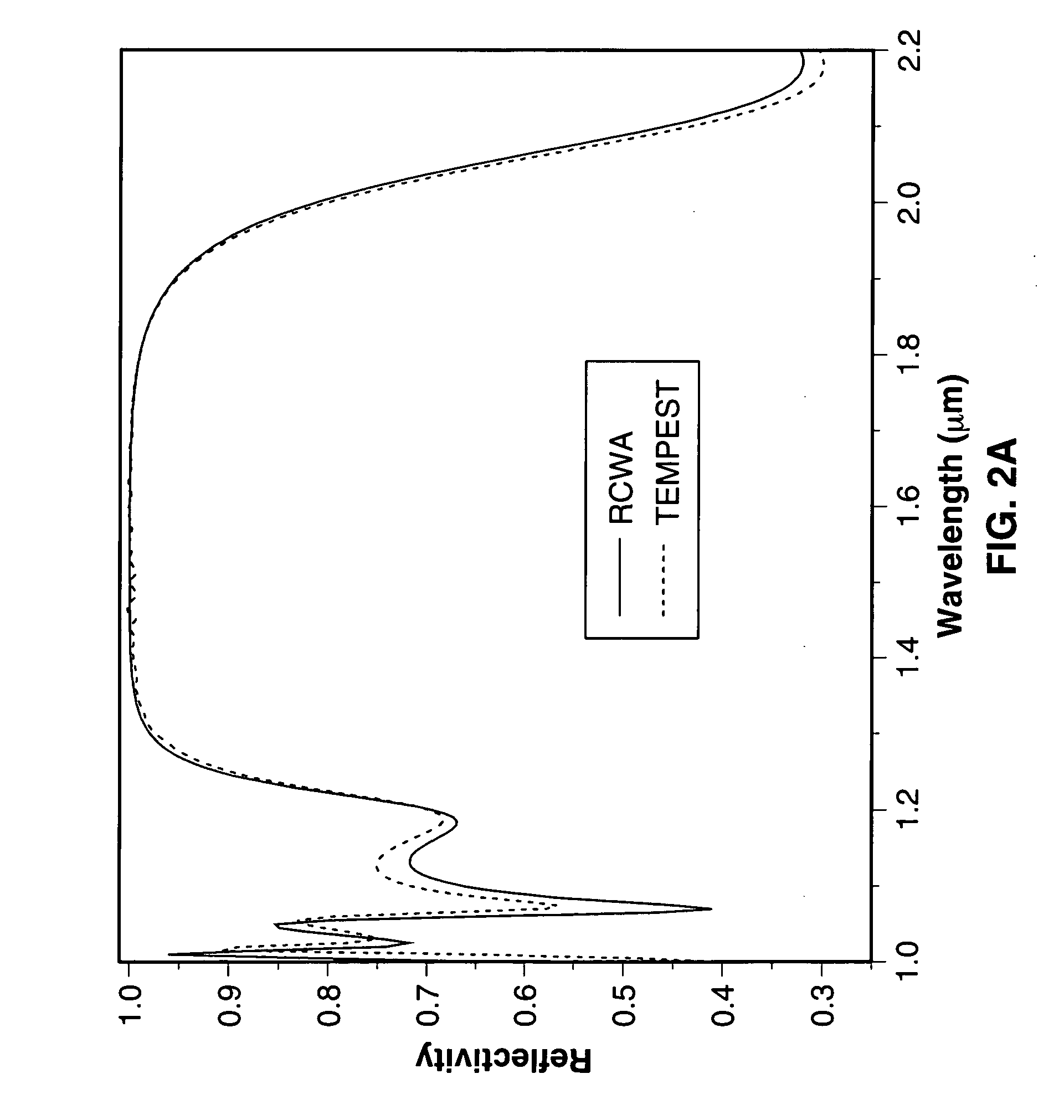
[0084]FIG. 2A through FIG. 2D illustrate simulated mirror reflectivity for linear polarized light in the direction perpendicular to the grating lines with results shown as a function of wavelength for the sub-wavelength grating structure shown in FIG. 1. FIG. 2A compares simulated reflectivity using both a Rigorous Coupled Wave Analysis (RCWA) and confirmed by finite difference time domain electromagnetic propagation using TEMPEST®. The two methods are in excellent agreement and both illustrate the broadband and highly reflective properties of the sub-wavelength grating. It can be seen that the sub-wavelength grating provides a very broadband mirror Δλ / λ>30%, with R>0.99, for wavelengths centered around 1.55 μm, over the range 1.33 μm to 1.80 μm, as depicted by FIG. 2A. The reflection bandwidth of the mirror is also very broad for a higher reflectivity R>0.999 (1.40 μm to 1.67 μm or Δλ / λ>17%).
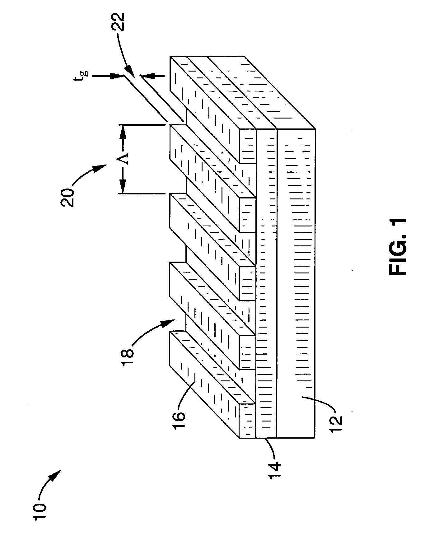
[0085] The parameters used in the simulation were: Si substrate (n=3.48), grating period Λ...
example 2
[0096] In order to demonstrate the functionality of the design, several single wavelength grating structures according to FIG. 1 were fabricated. The 1D grating structures were formed with stripes of high index material disposed on two low index layers. The high index material was poly-Si (nh)=3.48, and the low index material within the grating was air (n=1). The low index material under the grating was SiO2 with (nL)=1.47 and a thickness (tL)=0.58 μm and (tg)=0.4 μm. The grating period was varied from 0.7 μm to 0.9 μm and the grating duty cycle was varied 40-80%. The duty cycle is defined as the ratio of the width of the high index material to the total period length. Fabrication was conducted on a silicon wafer and e-beam lithography on PMMA was used for lift off of metal as to mask the top oxide layer, which was etched by RIE. The grating is polarization sensitive and light polarized along the grating lines will not see the band gap. However, if the grating has a two-dimensional ...
example 3
[0101] A simple one-dimensional (1D) grating was simulated to illustrate the scalability of the single wavelength grating structures and the dependence of reflectivity spectrum on various parameters. A very broadband mirror with reflectivity larger than 99%, is obtained over the range of 1.4 μm to 1.7 μm (Δλ / λ>19%). The simulation calculations were performed based on Rigorous
[0102] Coupled Wave Analysis (RCWA) and confirmed by time-domain electromagnetic propagation using TEMPEST®. The high index material was poly-Si (nh)=3.48, and the low index material within the grating was air (n=1). The low index material under the grating was SiO2 with (nL)=1.47 and a thickness (tL)=0.5 μm and (tg)=0.46 μm. The fill factor was 0.75 and the grating period was 0.7 μm. The index of refraction was considered constant along the coverage range.
[0103] It can be seen that the period of the grating in the simulation is sub-wavelength (but not half wavelength) and a scalable constant. Accordingly, the...
PUM
 Abstract
Description
Claims
Application Information


