Vertical deep ultraviolet light emitting diodes

Active Publication Date: 2010-12-16
NIITEK
View PDF9 Cites 40 Cited by
  • Summary
  • Abstract
  • Description
  • Claims
  • Application Information

AI Technical Summary

Benefits of technology

[0015]Another particular advantage of a preferred embodiment of the present invention is the abil

Problems solved by technology

A deficiency of LEDs with laterally conducting geometry is current crowding which results from forcing the current to travel laterally through a semiconductor with finite resistance prior to traveling vertically through the LE

Method used


Image

  • Vertical deep ultraviolet light emitting diodes
  • Vertical deep ultraviolet light emitting diodes
  • Vertical deep ultraviolet light emitting diodes

Examples


Embodiment Construction

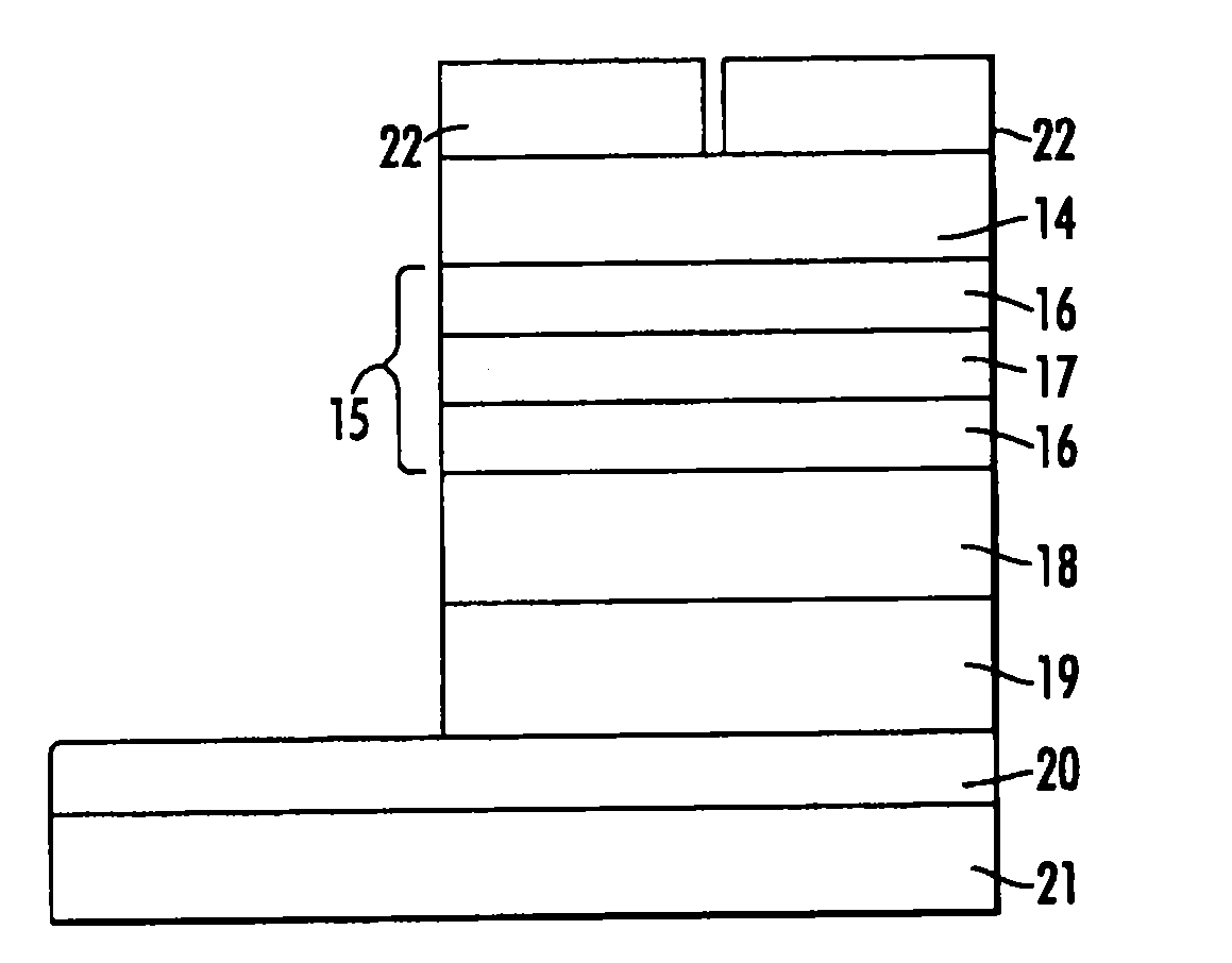
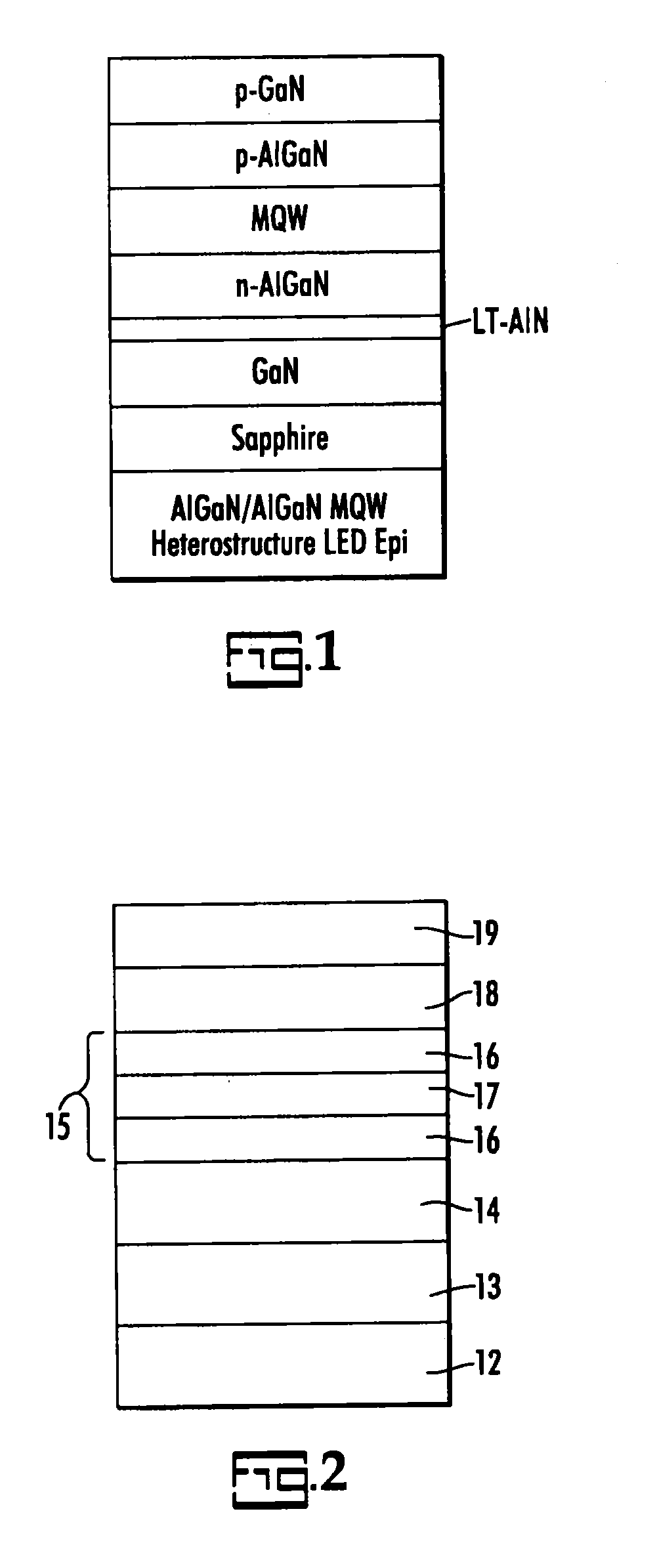
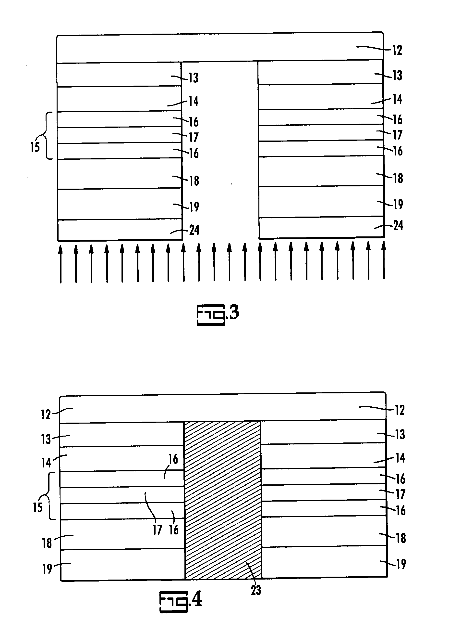
[0028]The present invention will be described with reference to the various figures forming an integral part of the disclosure. Throughout the various figures similar elements will be numbered accordingly.

[0029]The present invention provides an ultraviolet, more preferably a deep ultraviolet light, emitting device. Deep ultraviolet, when used herein, refers to a peak output wavelength from 200-365 nm.

[0030]It is well known to those skilled in the art that an active LED comprises semiconducting materials doped with impurities to form a p-n junction. Current flows from the p-side, or anode, to the cathode, or n-side, but not in the reverse direction. The wavelength of radiation is dependent on the band gap energy of the materials forming the p-n junction. Though not limited thereto the present invention is particularly well suited for use in nitride-based light emitting devices such as Group III-nitride based devices. “Group III nitride” refers to those semiconducting compounds formed...


PUM


Abstract

The invention is a vertical geometry light emitting diode capable of emitting light in the electromagnetic spectrum having a substrate, a lift-off layer, a strain relieved superlattice layer, a first doped layer, a multilayer quantum wells comprising alternating layers quantum wells and barrier layers, a second doped layer, a third doped layer and a metallic contact that is in a vertical geometry orientation. The different layers consist of a compound with the formula AlxlnyGa(1-x-y)N, wherein x is more than 0 and less than or equal to 1, y is from 0 to 1 and x+y is greater than 0 and less than or equal to 1. The barrier layer on each surface of the quantum well has a band gap larger than a quantum well bandgap. The first and second doped layers have different conductivities. The contact layer has a different conductivity than the third doped layer

Description

CROSS-REFERENCE TO RELATED APPLICATIONS[0001]This application claims priority to pending U.S. Provisional Patent Application No. 60 / 852,672 filed Oct. 18, 2006 which is incorporated herein by reference.BACKGROUND[0002]The present invention is directed to a vertical geometry light emitting diode. More specifically, the present invention is related to a vertical geometry light emitting diode which emits ultraviolet, more preferably deep ultraviolet light.[0003]Ultraviolet (UV) light emitting diodes (LEDs) are typically grown on electrically insulating substrates such as sapphire or bulk aluminum nitride. This requires the metallic contacts, often referred to as an anode and cathode, to be located on the same side of the final epitaxial wafer to allow current to pass through the diode. This geometry is typically referred to as a laterally conducting geometry since the electrodes are laterally displaced relative to each other. Non-exhaustive examples of lateral displaced geometry LEDs a...

Claims


Application Information

Patent Timeline
IPC IPC(8): H01L33/06H01L21/18H01L33/00H01L33/32
CPCB82Y20/00H01L33/32H01L33/06H01L33/0079H01L33/0093H01L33/02
Inventor KHAN, ASIF
Owner NIITEK
Why Eureka
Try Eureka