Metallizing device and method

a technology of metal contact and metallization paste, which is applied in the direction of photovoltaic energy generation, ion implantation coating, coating, etc., can solve the problems of evaporation of solvents found in metallization paste, high resistivity of materials, and limited height/width form factor of metallization, so as to reduce the proportion of binders, increase the viscosity, and increase the viscosity

Inactive Publication Date:
View PDF6 Cites 10 Cited by
  • Summary
  • Abstract
  • Description
  • Claims
  • Application Information

AI Technical Summary

Benefits of technology

[0036]This increase in the viscosity of the metallization paste as compared with the metallization pastes used in the methods of the prior art, may be obtained by reducing the proportion of binders in the composition of the metallization paste. This increase in the viscosity may also be obtained by adding a flow additive, for example a thixotropic agent.
[0037]By using such a metallization paste, it is for example possible to make narrow and high conductors, reducing the surface area occupied on a front side of a photovoltaic cell as compared with the conductors made according to the methods of the prior art. This therefore leads to an increase in the conversion yield of a photovoltaic cell which is thereby metallized at the front side, because of an increase in the current produced by the cell (less shadowing formed by the metallizations on the front side) and of the improvement of the form factor (decrease of the series resistance of these metallizations). Also, producing metallizations on the rear side of a photovoltaic cell with this method, object of the present invention, is particularly useful when constraints on resistance require the making of narrow conductors.
[0038]By using a paste with a higher viscosity, with limited spreading of this paste after its deposit, it is possible to obtain narrower and thicker conductors for a same transferred volume of paste.
[0039]By using such a metallization paste, the thickness of the obtained metallization after drying is larger because of the reduction in volume loss related to evaporation of the solvent(s) present in the binders. Further, baking of the paste is facilitated by the reduction in the amount of resin to be burnt (case of the pastes of the prior art dedicated to the method for metallizing photovoltaic cells with high temperature baking).

Problems solved by technology

However, these metallizations must have a sufficient section so as to limit the series resistances, which imposes a thickness all the larger since the conductors are narrower and the resistivity of the material is high.
Screen printing is an economical technique because of its high productivity, but leads to a limited height / width form factor for metallizations.
Problems related to evaporation of the solvents found in the metallization paste also occur during screen printing.
This evaporation may be an obstacle for properly metallizing the semiconductor device.
Further, during screen printing, the metallization paste is subject to shear movements due to scraping, involving a reduction in the viscosity of the paste and causing an untimely spreading of this metallization paste.

Method used


Image

  • Metallizing device and method
  • Metallizing device and method
  • Metallizing device and method

Examples


first embodiment

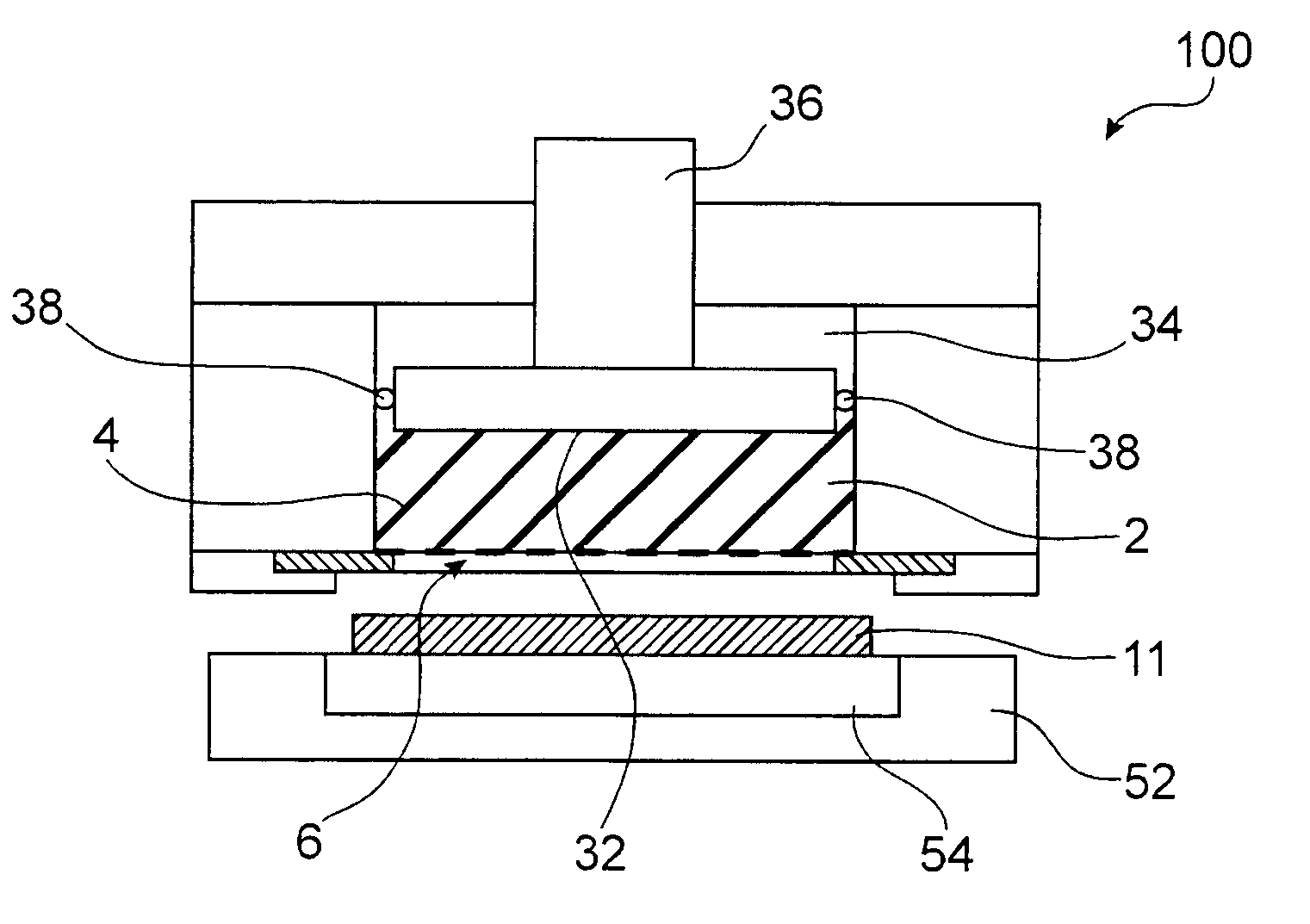
[0050]First of all, reference will be made to FIG. 1A which illustrates a metallization device 100 according to a

[0051]The metallization device 100 includes a closed enclosure 2 of variable volume intended to contain the metallization paste 4. In this first embodiment, a semiconductor device 11 intended to be metallized by the metallization device 100 is photovoltaic cell.

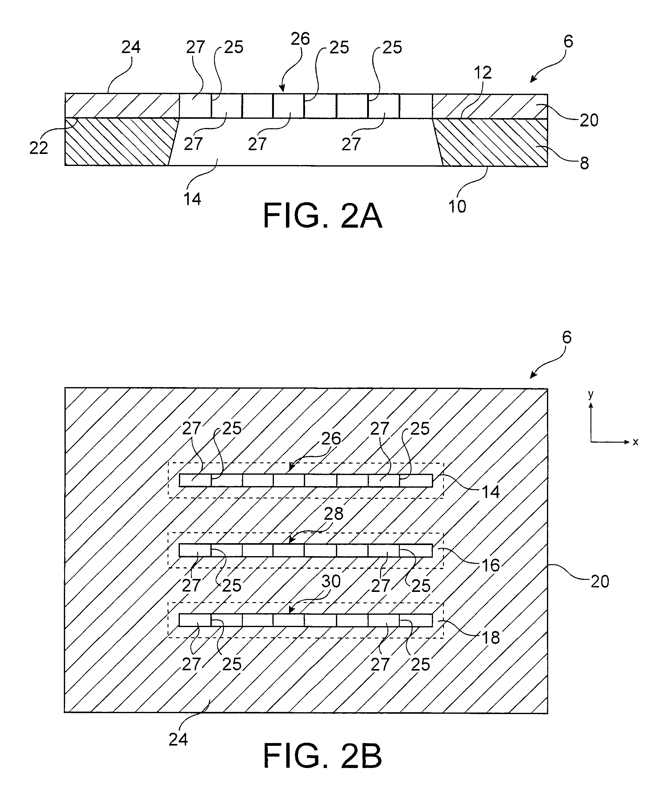
[0052]A printing screen 6 forms one of the walls of the enclosure 2. This printing screen 6 may for example be a screen of the stencil or web type. In this first embodiment, the printing screen 6 is a dual layer screen as described later on in connection with FIGS. 2A and 2B.

[0053]In the metallization device 100, the closed enclosure 2 is made in such a way that the application of a force or pressure on a mobile sealed wall 32 of the enclosure 2 opposite to the wall formed by the printed screen 6 causes a reduction in the volume of the enclosure 2. With this volume reduction of the enclosure 2 it is possible to cau...

second embodiment

[0077]FIG. 4 illustrates a metallization device 400 according to a This device 400 includes an upper portion formed by a plate 46, bound to a support 52 intended to receive the semiconductor device 11.

[0078]The metallization device 400 includes a lower portion including a solid reservoir formed by the sidewalls 50 and a component 58 forming a bottom wall, the sidewalls 50 being translationally mobile relatively to the component 58. A closed enclosure 2 formed by a sealed membrane 40 is positioned in the solid reservoir. A plate 60 supports the components of the lower portion of the metallization device 400. Regulation means 56, such as a plate based on a heat conducting material including an integrated piping network allowing circulation of a temperature-regulated fluid, allows the temperature to be controlled inside the enclosure 2 and to be regulated in order to, for example, temporarily decrease the viscosity of the paste so as to facilitate injection by raising the paste to a t...


PUM

PropertyMeasurementUnit
viscosityaaaaaaaaaa
temperatureaaaaaaaaaa
viscosityaaaaaaaaaa

Abstract

A metallization device configured to metallize a semiconductor device, including: a closed enclosure of variable volume configured to contain a metallization paste, a screen for screen printing forming a wall of the enclosure integral with the other walls of the enclosure, configured to be in contact with the semiconductor device during its metallization, and a mechanism applying uniform pressure over a mobile sealed wall of the enclosure opposite to the wall formed by the printing screen and reducing the volume of the enclosure. The volume reduction of the enclosure is configured to cause the metallization paste to uniformly pass through the printing screen.

Description

TECHNICAL FIELD AND PRIOR ART[0001]The invention relates to the metallization or production of metal contacts, of semiconductor devices and more particularly to the metallization of photovoltaic cells.[0002]Photovoltaic cells include metallizations either made on the front side, i.e. the side intended to receive light radiation, and on the rear side, or exclusively on the rear side (RCC << Rear Contact Cell >> or IBC << Interdigitated Back Contact >> cells). In order for the cell to receive maximum radiation, the metallizations made on the front side are preferably narrow in order to reduce as much as possible the occupied surface area on the front side of the cell, i.e. to minimize the shadowing on this front side. However, these metallizations must have a sufficient section so as to limit the series resistances, which imposes a thickness all the larger since the conductors are narrower and the resistivity of the material is high.[0003]Metallization by scree...

Claims


Application Information

Patent Timeline
Patent Type & Authority Applications(United States)
IPC IPC(8): H01L31/18B05C11/02
CPCB41F15/00B41F15/36Y02E10/50H01L31/18H01L31/022425
Inventor BETTINELLI, ARMAND
Why Eureka
Try Eureka