Photodiode and other sensor structures in flat-panel x-ray imagers and method for improving topological uniformity of the photodiode and other sensor structures in flat-panel x-ray imagers based on thin-film electronics

a flat-panel x-ray imager and sensor technology, applied in the direction of x/gamma/cosmic radiation measurement, instruments, radioation controlled devices, etc., can solve the problems of introducing additional, difficult to yield and costly production of devices, and limiting the range of imagers

Active Publication Date: 2010-12-23
RGT UNIV OF MICHIGAN
View PDF10 Cites 101 Cited by
  • Summary
  • Abstract
  • Description
  • Claims
  • Application Information

AI Technical Summary

Problems solved by technology

In the case of c-Si technology, pixilated imaging arrays (such as charge coupled devices (CCDs), CMOS sensors, active pixel sensors, and passive pixel sensors) are ultimately limited by the size of the silicon wafers used for fabrication, currently up to ˜300 mm.
While such devices have been made with dimensions as large as ˜20 cm by 20 cm, these devices are hard to yield and costly to produce.
Also, while large area devices can be made by tiling small area c-Si arrays, this introduces additional, significant engineering problems, challenges, and costs.
While simple array designs incorporate only a single switch per pixel for purposes of addressing, more complex designs can include additional circuit elements in the pixel that serve to improve the performance and / or extend imager capabilities.
Of course, the imaging signals can be sampled from two or more consecutive rows at a time, which decreases the read-out time, but at the cost of reduced spatial resolution.
Furthermore, the address and bias lines must be sufficiently wide to limit the electrical resistance along these lines (since high resistance would negatively affect the temporal and / or electrical operation of the array, as well as possibly decrease signal-to-noise performance).
In addition, the gaps must not be so narrow as to lead to unintended contact (and thus electrical shorting) between pixel elements or to high levels of parasitic capacitance (which can degrade the signal-to-noise ratio and the temporal performance).
The challenge of maintaining a large optical fill factor becomes more difficult as pixel pitch decreases, since the area occupied by the address lines, gaps, and addressing TFT consumes an ever-greater fraction of the pixel area.

Method used


Image

  • Photodiode and other sensor structures in flat-panel x-ray imagers and method for improving topological uniformity of the photodiode and other sensor structures in flat-panel x-ray imagers based on thin-film electronics
  • Photodiode and other sensor structures in flat-panel x-ray imagers and method for improving topological uniformity of the photodiode and other sensor structures in flat-panel x-ray imagers based on thin-film electronics
  • Photodiode and other sensor structures in flat-panel x-ray imagers and method for improving topological uniformity of the photodiode and other sensor structures in flat-panel x-ray imagers based on thin-film electronics

Examples


Embodiment Construction

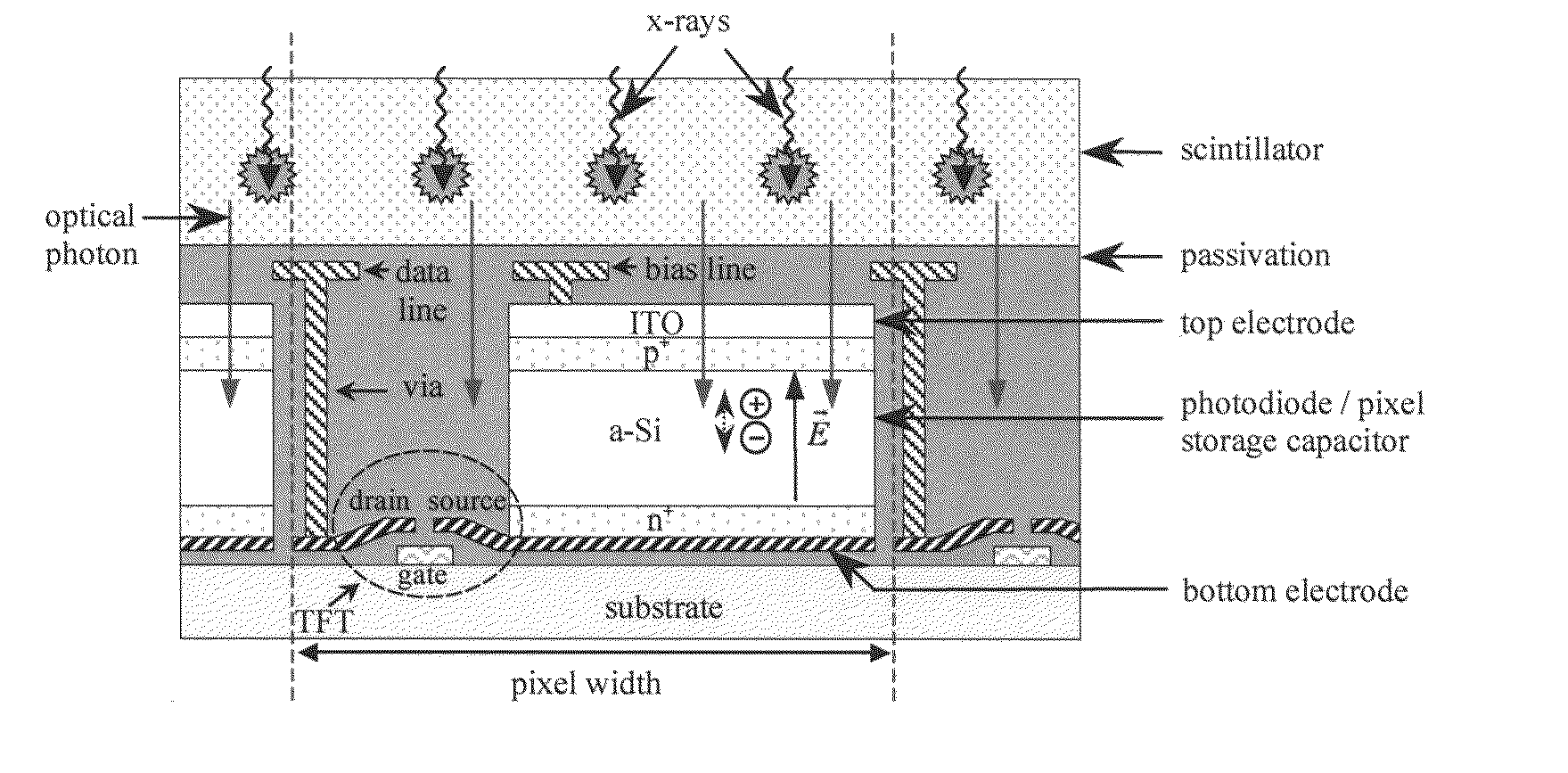
[0091]The incorporation of out-of-plane photodiode structures into the pixel design of indirect detection active matrix arrays provides a mechanism for significantly improving optical fill factor. In the case of the implementation of continuous photodiode structures, optical fill factors as large as unity, corresponding to the entire area of the pixel, are possible. Such optical fill factor improvements result from eliminating the competition for pixel area between the photodiode and other pixel elements such as the addressing TFT, address lines and gaps.

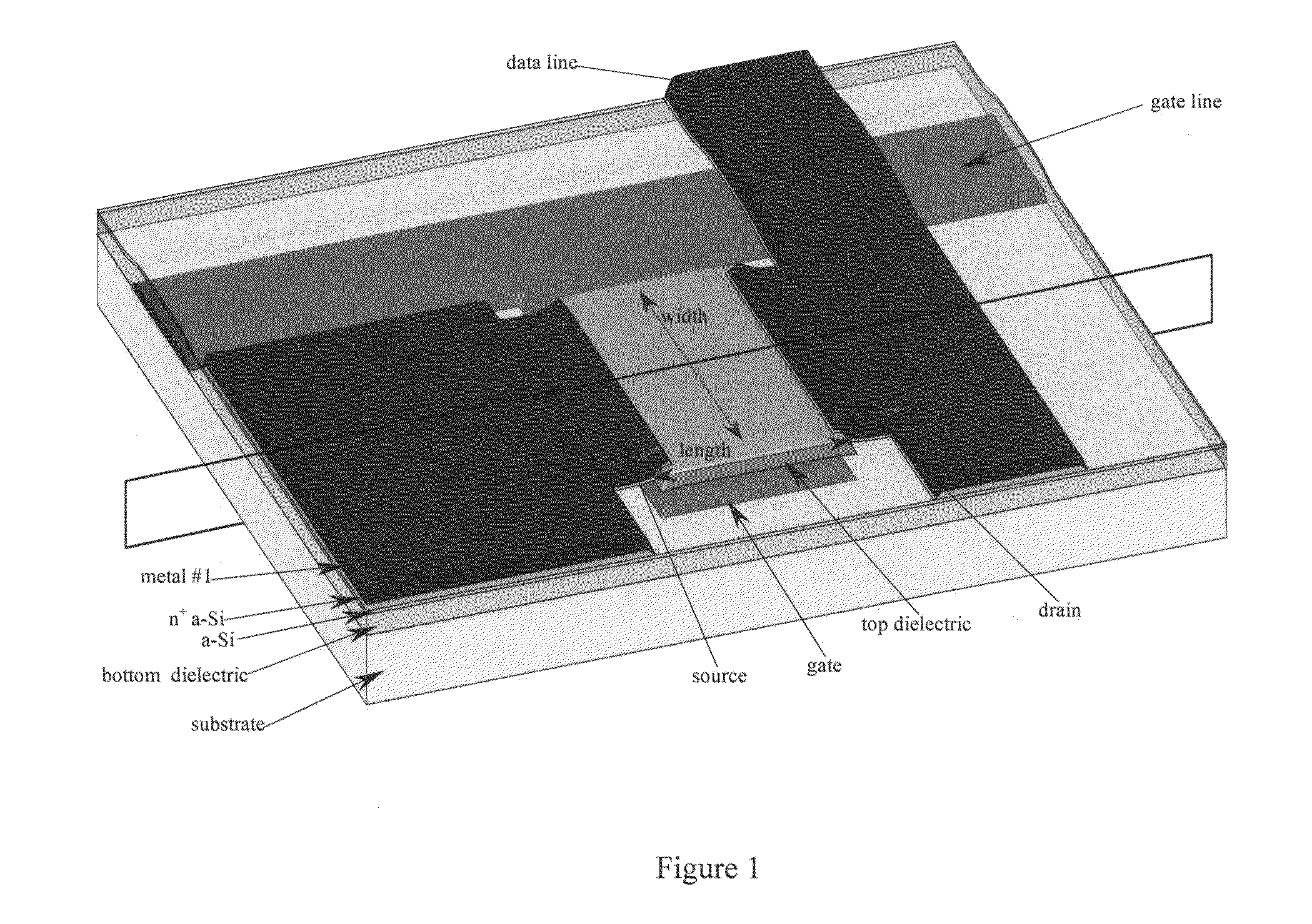
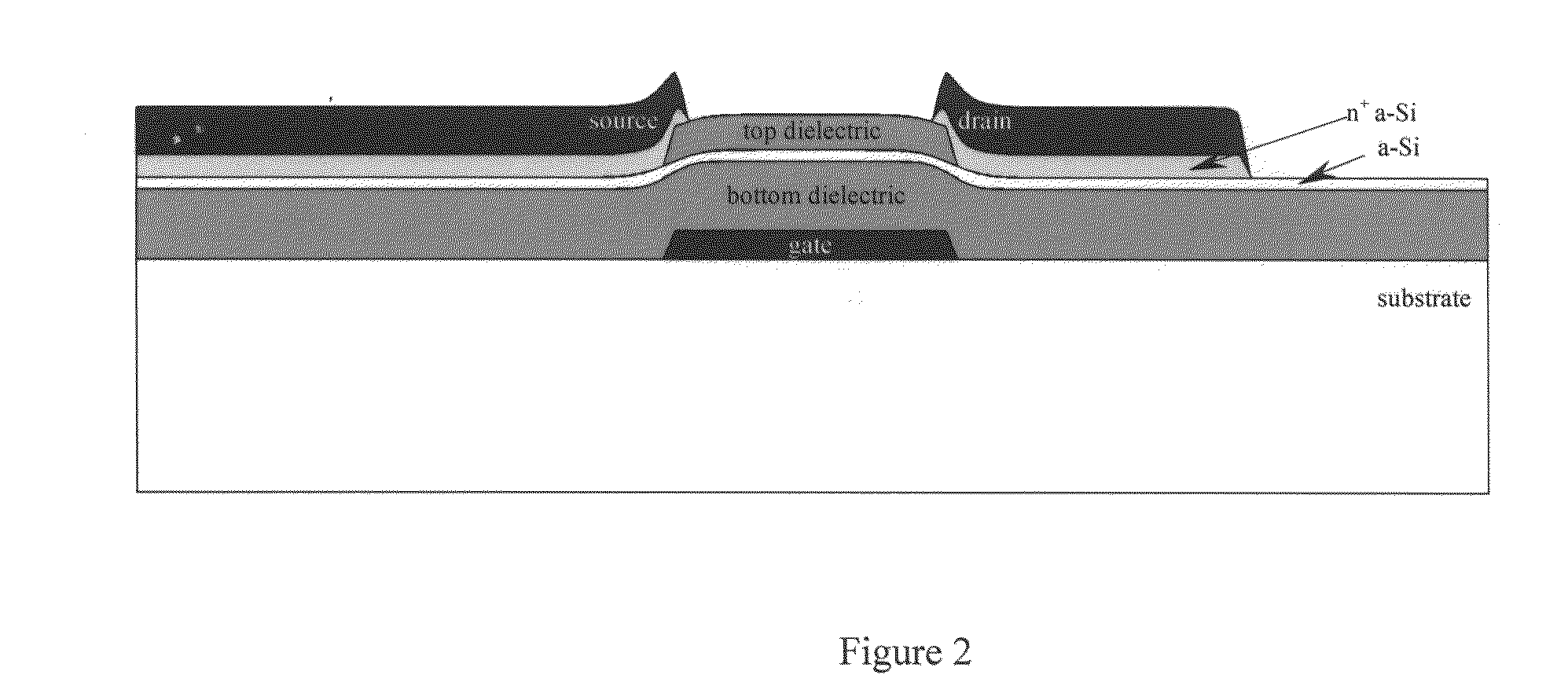
[0092]Out-of-plane photodiode structures also make it possible to introduce additional elements to the pixels (such as TFTs, diodes, capacitors and resistors, as well as vias, traces, control lines, address lines and ground planes), thereby making more complex pixel circuits possible. As in the case of active matrix arrays, these additional elements would reside in a separate plane from that of the photodiode and therefore would not...


PUM


Abstract

A radiation sensor including a scintillation layer configured to emit photons upon interaction with ionizing radiation and a photodetector including in order a first electrode, a photosensitive layer, and a photon-transmissive second electrode disposed in proximity to the scintillation layer. The photosensitive layer is configured to generate electron-hole pairs upon interaction with a part of the photons. The radiation sensor includes pixel circuitry electrically connected to the first electrode and configured to measure an imaging signal indicative of the electron-hole pairs generated in the photosensitive layer and a planarization layer disposed on the pixel circuitry between the first electrode and the pixel circuitry such that the first electrode is above a plane including the pixel circuitry. A surface of at least one of the first electrode and the second electrode at least partially overlaps the pixel circuitry and has a surface inflection above features of the pixel circuitry. The surface inflection has a radius of curvature greater than one half micron.

Description

CROSS REFERENCE TO RELATED APPLICATIONS[0001]This application is related to and claims priority under 35 U.S.C. 119(e) to U.S. provisional patent application 61 / 213,530, filed Jun. 17, 2009, entitled “PHOTODIODE AND OTHER SENSOR STRUCTURES IN FLAT-PANEL X-RAY IMAGERS AND METHOD FOR IMPROVING TOPOLOGICAL UNIFORMITY OF THE PHOTODIODE AND OTHER SENSOR STRUCTURES IN FLAT-PANEL X-RAY IMAGERS BASED ON THIN-FILM ELECTRONICS,” the entire disclosures of which are hereby incorporated by reference.STATEMENT REGARDING FEDERALLY SPONSORED RESEARCH OR DEVELOPMENT[0002]This invention was made with government support under EB000558 awarded by the National Institutes of Health. The government has certain rights in the invention.BACKGROUND OF THE INVENTION[0003]1. Field of the Invention[0004]The present invention pertains generally to devices designed to detect incident ionizing radiation in order to form images.[0005]2. Discussion of the Background[0006]In the field of x-ray imaging, imagers based o...

Claims


Application Information

Patent Timeline
Patent Type & Authority Applications(United States)
IPC IPC(8): G01T1/208H01L31/18G01T1/20H01L31/102
CPCH01L27/1462H01L27/14658H01L27/14687H01L27/14689G01T1/208H01L27/14632H01L27/14663G01T1/241H01L31/105H01L27/146H01L27/14605G01T1/20184H01L27/14612H01L27/14636
Inventor ANTONUK, LARRY E.
Owner RGT UNIV OF MICHIGAN
Why Eureka
Try Eureka