Active device array substrate

a technology of active devices and arrays, applied in the field of substrates, to achieve the effect of significantly reducing parasitical capacitors and increasing aperture ratios

Active Publication Date: 2010-12-30
AU OPTRONICS CORP
View PDF9 Cites 10 Cited by
  • Summary
  • Abstract
  • Description
  • Claims
  • Application Information

AI Technical Summary

Benefits of technology

[0009]The present invention provides an active device array device which significantly increases the a

Problems solved by technology

Therefore, it is an important issue to prevent a light leakage w

Method used


Image

  • Active device array substrate
  • Active device array substrate
  • Active device array substrate

Examples


first embodiment

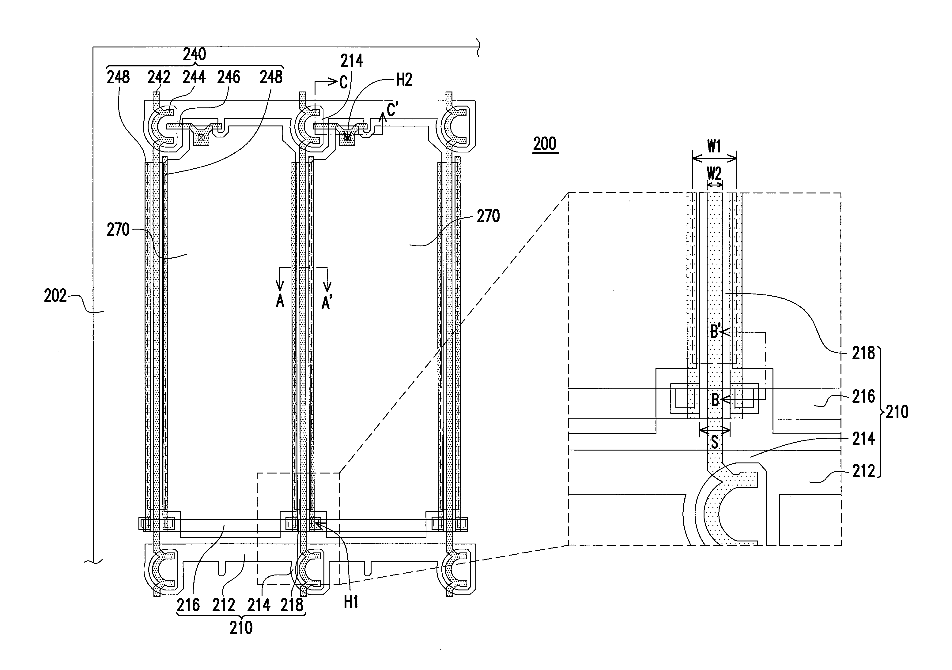
[0033]FIG. 2 is a local top view of an active device array substrate of the first embodiment of the present invention. FIG. 3A is local cross-sectional view of the active device array substrate in FIG. 2 applied to a liquid crystal display, wherein FIG. 3A is cross-sectioned at a position corresponding to the position where the active device array substrate 200 is cross-sectioned along the section line AN in FIG. 2. Referring to FIGS. 2 and 3A, the active device array substrate 200 of this embodiment includes a substrate 202, a first patterned conductive layer 210, a dielectric layer 230, a second patterned conductive layer 240, a passivation layer 260, and a plurality of pixel electrodes 270.

[0034]Referring to FIGS. 2 and 3A, the first patterned conductive layer 210 is disposed on the substrate 202. The first patterned conductive layer 210 includes a plurality of scan lines 212, a plurality of gates 214 connected with the scan lines 212, a plurality of common lines 216, and a plura...

second embodiment

[0047]FIG. 4 is a local top view of an active device array substrate of the second embodiment of the present invention. Referring to FIG. 4, an active device array substrate 400 of this embodiment is similar to the active device array substrate 200 of the first embodiment; however, in the pixel units of the active device array substrate 400 of this embodiment, the storage capacitor is in a storage capacitor on scan lines 212 (Cst on scan line) structure. For clearer illustration, identical reference numerals are used on elements identical with those in the first embodiment.

[0048]FIG. 5 is a cross-sectional schematic view along the section line BB′ in FIG. 4. Referring to FIG. 5, in this embodiment, the first contact holes H1 of the dielectric 230 is located above the scan lines 212. In other words, the first contact holes H1 exposes a portion of the scan lines 212, respectively. Moreover, each of the strip capacitance electrodes 248 is electrically connected to one of the scan lines...


PUM


Abstract

An active device array substrate including a first patterned conductive layer, a dielectric layer, a second patterned conductive layer, a passivation layer and pixel electrodes is provided. The first patterned conductive layer includes scan lines, common lines, gates and strip floating shielding patterns. The dielectric layer covering the first patterned conductive layer has first contact holes which expose a portion of the common lines, respectively. The second patterned conductive layer includes data lines, sources, drains and strip capacitance electrodes. Each strip capacitance electrode is electrically connected to one of the common lines through one of the first contact holes. A gap is formed between each data line and one strip capacitance electrode, and the strip floating shielding patterns are disposed under the data lines, the gap and the strip capacitance electrodes. Each pixel electrode is electrically connected to one of the drains through one of the second contact holes.

Description

CROSS-REFERENCE TO RELATED APPLICATION[0001]This application claims the priority benefit of Taiwan application serial no. 98122146, filed Jun. 30, 2009. The entirety of the above-mentioned patent application is hereby incorporated by reference herein and made a part of specification.BACKGROUND OF THE INVENTION[0002]1. Field of the Invention[0003]The present invention relates to a substrate, and particularly to an active device array substrate.[0004]2. Description of Related Art[0005]Among various flat panel displays (FPD), Liquid Crystal Display (LCD) has become a mainstream in the market due to its advantages such as high space utilization, low power consumption, absence of radiation, and low electromagnetic interference.[0006]FIG. 1A is a perspective view of a conventional liquid crystal display. Referring to FIG. 1A, the conventional liquid crystal display 100 has an active device array substrate 110, an opposite substrate 120, a liquid crystal layer 130 sandwiched between the ac...

Claims


Application Information

Patent Timeline
IPC IPC(8): H01L27/12
CPCG02F1/134363G02F1/136213H01L27/124H01L27/12G02F1/136286
Inventor LIU, CHU-YUSHIH, MING-HUNGWU, CHOU-CHINCHEN, I-CHUN
Owner AU OPTRONICS CORP
Why Eureka
Try Eureka