Display device and driving method

a technology of a display device and a driving method, applied in the field of display devices and driving methods, can solve the problems of affecting the detection speed of contacts, so as to achieve the effect of minimal latency and high detection speed

Active Publication Date: 2010-12-30
JAPAN DISPLAY WEST
View PDF7 Cites 63 Cited by
  • Summary
  • Abstract
  • Description
  • Claims
  • Application Information

AI Technical Summary

Benefits of technology

[0021]The present invention provides a display device having a contact detection function...

Problems solved by technology

Users may perceive a delay from when they touch the detection surface to when the contact is detected.
The longer the delay, the ...

Method used


Image

  • Display device and driving method
  • Display device and driving method
  • Display device and driving method

Examples


first embodiment

1. First Embodiment

Basic Configuration for Contact Detection and Operation

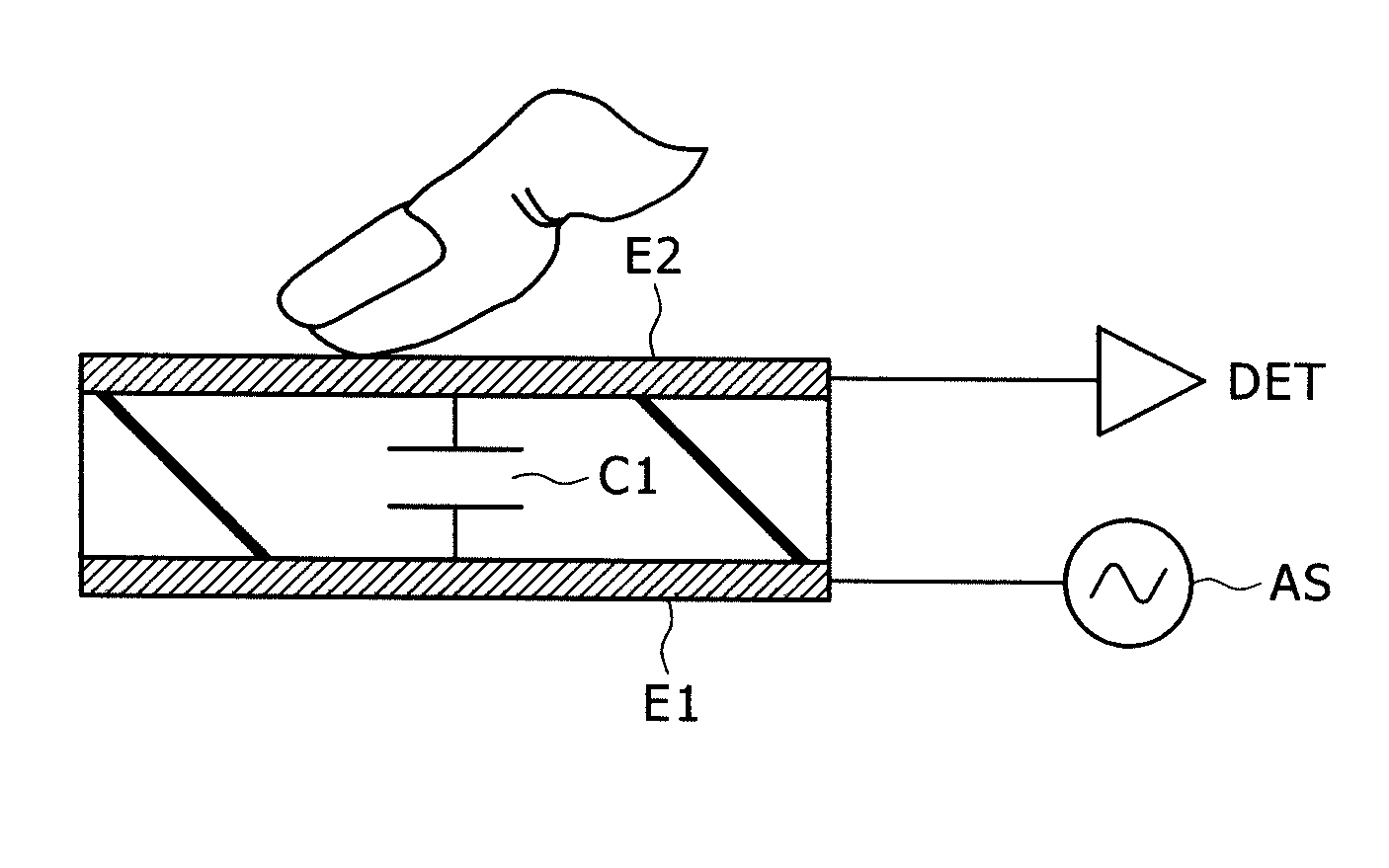
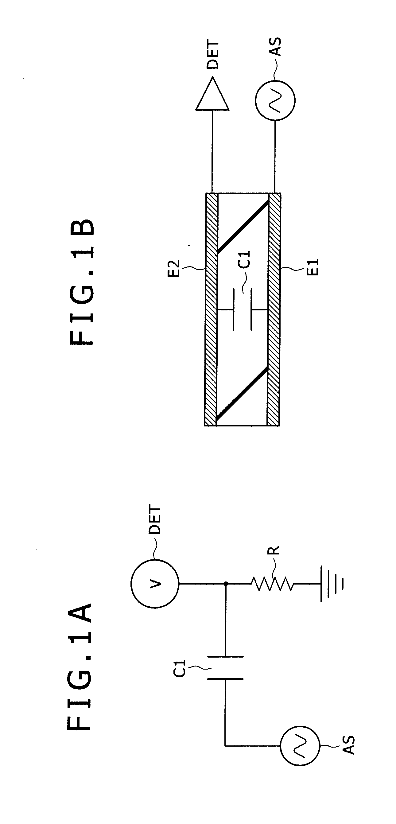
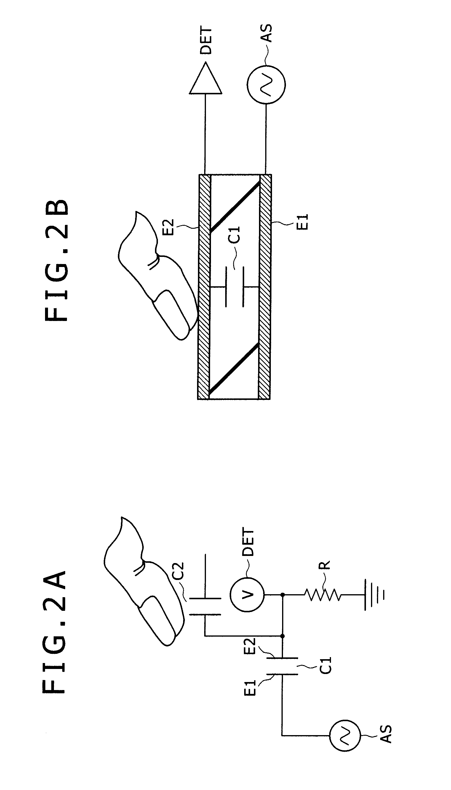
[0043]A description will be given first of the basics of electrostatic capacitance-based contact detection with reference to FIGS. 1A to 3C as a precondition in the first embodiment (condition common to this and other embodiments).

[0044]FIGS. 1A and 2A are equivalent circuit diagrams of a touch sensor section, and FIGS. 1B and 2B structural diagrams (schematic cross-sectional views) of the touch sensor section. Here, FIGS. 1A and 1B illustrate a case in which an object to be detected or a finger is not in proximity to the sensor, and FIGS. 2A and 2B a case in which a finger is in proximity to or contact with the sensor.

[0045]The touch sensor section illustrated in the figures is an electrostatic capacitance touch sensor that includes a capacitive element as illustrated in FIGS. 1B and 2B. More specifically, a capacitive element (electrostatic capacitance) C1 is formed with a dielectric D and a pair of electrod...

second embodiment

2. Second Embodiment

[0102]As described above, in the case of the contact detection scan performed at triple speed or more, the contact detection scan passes the display scan at some points. When the write pixel line WPL being displayed is driven by the contact detection scan (detection scanning and driving) at the same time, problems such as noise in the video signal may occur due to the contact detection drive signal. In this case, dim stripes may be constantly observed at locations associated with the points where the passing takes place, thus resulting in degradation of the display quality.

[0103]The present embodiment proposes two approaches to prevent this degradation of the display quality.

[0104]The first approach is to skip at least one drive electrode DE (or more) at points where the drive electrode DE subjected to the detection scan passes that subjected to the display scan or before and after these points. This approach is a so-called discretely reducing method adapted to d...

third embodiment

3. Third Embodiment

[0113]FIG. 12 is a diagram illustrating a driving method according to a third embodiment.

[0114]This driving method performs the detection scan nearly two times faster than the display scan. Here, if border scanning is performed with the arrangement pitch of the drive electrodes DE in the Y direction being k-fold the pixel pitch in the Y direction, the larger the drive electrode pitch is than the pixel pitch, the farther apart the double speed of the display scan is from the detection scan speed. It should be noted, however, that the value k is significantly smaller than the vertical pixel count. As a result, the difference in speed is small. Therefore, the display scan and detection scan can be performed almost at the same frequency. This is advantageous in that the configuration of the scan drive section 9 or clock generating circuit can be simplified. It should be noted, however, that interlaced scan must be used for the display scan.

[0115]It can be said that th...


PUM


Abstract

Disclosed herein is a display device, including: a display surface; a display functional layer adapted to control the display of a screen viewed from outside the display surface; a drive control section operable to perform display scanning and driving adapted to scan and drive, in the one direction, the plurality of drive electrodes, and also operable to perform, a plurality of times and for M display screens, detection scanning and driving adapted to continuously scan and drive all or part of the plurality of drive electrodes within the period of time; and a plurality of sensor lines arranged in a direction other than the one direction to be separate from each other, which produce an electrical change if an object to be detected comes in contact with or proximity to the display surface while the drive control section performs the detection scanning and driving.

Description

[0001]The present application claims priority to Japanese Patent Application No. JP 2009-155194 filed with the Japan Patent Office on Jun. 30, 2009, the entire content of which is hereby incorporated by reference.BACKGROUND OF THE INVENTION[0002]1. Field of the Invention[0003]The present invention relates to a display device capable of detecting an object such as user's finger or pen coming in contact with or proximity to the display surface, and to a driving method of the same.[0004]2. Description of the Related Art[0005]Three methods, namely, optical method, resistance film method and electrostatic capacitance method, are known as the contact detection methods of a touch panel.[0006]In order to associate the electrical change resulting from an object coming in contact or proximity with positional information, on the other hand, a number of wirings are required that are arranged in a matrix form and combined in such a manner as to allow identification of positions. An enormous numb...

Claims


Application Information

Patent Timeline
IPC IPC(8): G09G5/00
CPCG02F1/13338G02F1/136286G06F3/0412G06F3/044G09G5/18G09G2310/02G09G2320/0252G09G2340/0435G09G3/3674G09G3/3648G06F3/0445G06F3/0446
Inventor NOGUCHI, KOUJINAKANISHI, TAKAYUKIISHIZAKI, KOJITERANISHI, YASUYUKITAKEUCHI, TAKEYA
Owner JAPAN DISPLAY WEST
Why Eureka
Try Eureka