Secure test-for-yield chip diagnostics management system and method

a test-for-yield chip and management system technology, applied in the field of secure test-for-yield chip diagnostic management system and method, can solve the problems of poor error analysis situation, fabricator company would typically have very little information, and companies that design chips will typically not give detailed chip design information to fabricator companies

Active Publication Date: 2010-12-30
TESEDA CORP
View PDF32 Cites 29 Cited by
  • Summary
  • Abstract
  • Description
  • Claims
  • Application Information

AI Technical Summary

Benefits of technology

[0005]This invention resolves the problem that arises when the fabricators or the production engineers find an error or failure but do not have enough information to correctly diagnose the cause the error or failure. This occurs more often when the fabricators and designers are at different companies than when the fabricators and designers are at the same company. Without more information, fabricators might be inclined to believe that problems arise from designs, while designers might be inclined to believe that a problem is caused by the fabricator. The present invention allows resolution such problems.
[0007]This invention provides a secure information exchange, so the fabricator can quickly discover a physical location where design or production flaws might be present. Scan logs provide logical information, which allows the physical location of the failure to be determined. Previously, the fabricator would have to go to the original designer to obtain information to locate the flaw, which could take many months or worst cases the designer would not release the information at all.

Problems solved by technology

Companies that design chips will typically not give detailed chip design information to the fabricator company.
As a result, when a manufactured device failure occurs, the fabricator company would typically have very little information to determine whether the failure is the result of a design flaw or a fabrication error because the fabricator company might have no design information other than the manufacturing mask or masks.
The error analysis situation is much worse at production test, because only the pattern and design information are known.
Without more information, fabricators might be inclined to believe that problems arise from designs, while designers might be inclined to believe that a problem is caused by the fabricator.
If no manufacturing problem is identified, then a design problem could be the cause of failure.
Previously, the fabricator would have to go to the original designer to obtain information to locate the flaw, which could take many months or worst cases the designer would not release the information at all.

Method used


Image

  • Secure test-for-yield chip diagnostics management system and method
  • Secure test-for-yield chip diagnostics management system and method
  • Secure test-for-yield chip diagnostics management system and method

Examples


Embodiment Construction

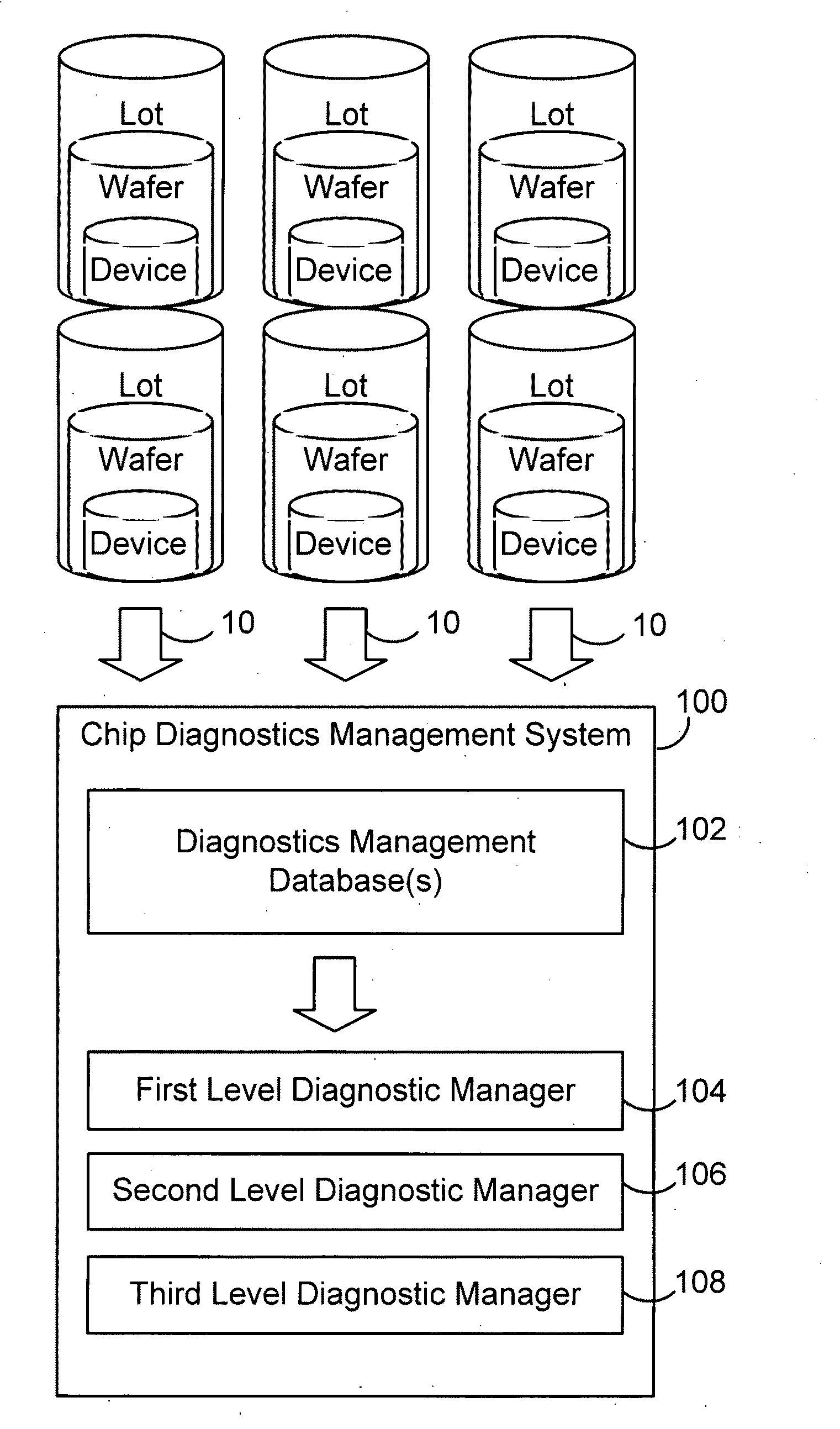
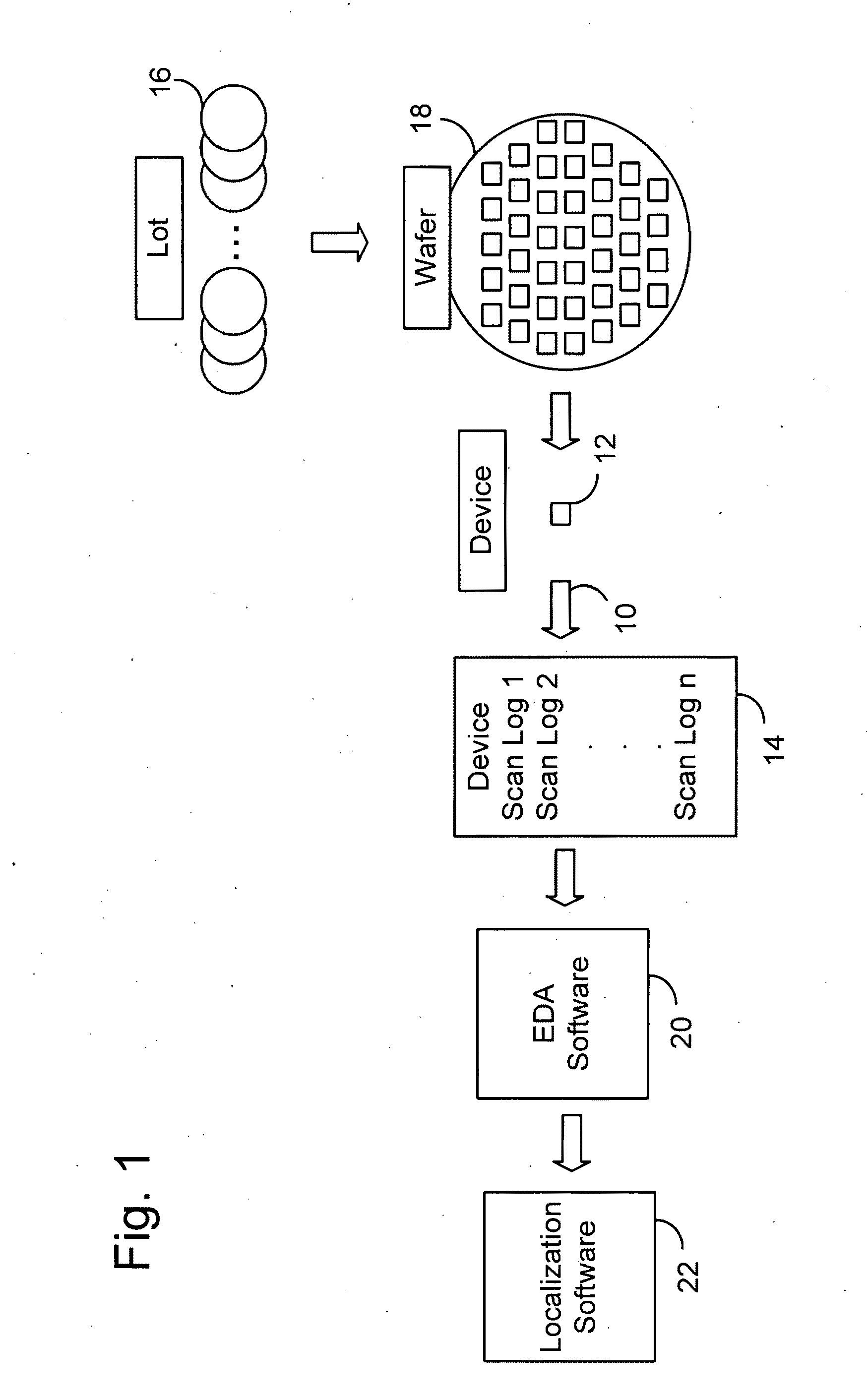
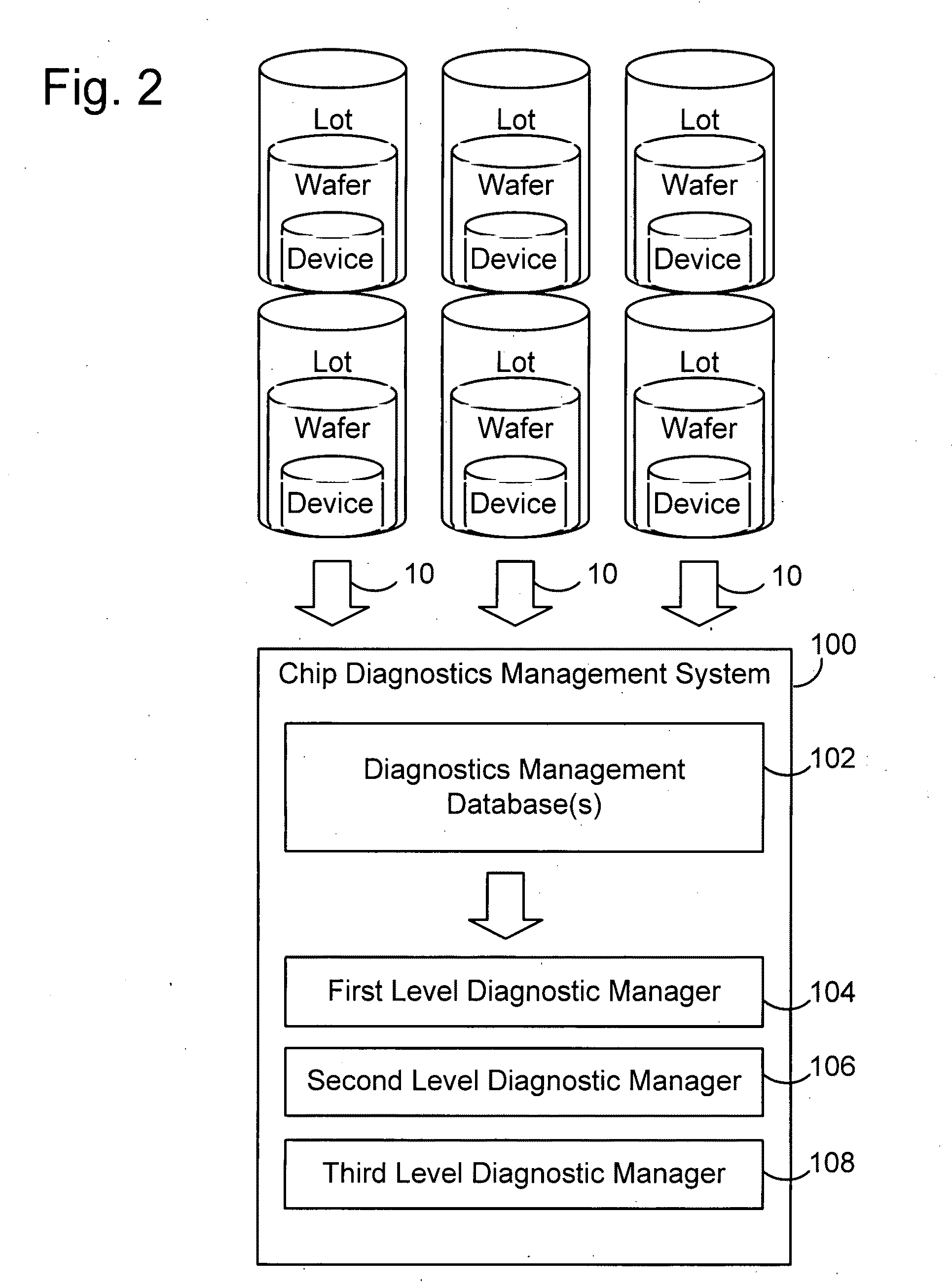
[0016]FIG. 1 is a block diagram generally illustrating prior art data flow in chip 10Diagnostics Amanagement Databasefailure analysis and diagnostics. Failure data 10 indicating defects or failures in each manufactured integrated circuit device 12 are obtained during production tests (e.g., with wafer probes) and stored in scan logs 14. Devices 12 are manufactured in lots 16 of wafers 18. The failure data are analyzed, such as by the electronic design automation (EDA) software 20 used to design devices 12, to identify logical defects 22 that correspond to the failure data 10 in a device 12. Localization software 24, such as that described in U.S. Pat. No. 6,185,707 for “IC Test Software System for Mapping Logical Functional Test Data of Logic Integrated Circuits to Physical Representation,” determines physical locations in devices that correspond to the failure data, thereby allowing localized viewing of the locations to diagnose the cause of the failures.

[0017]The process of diagno...


PUM


Abstract

A chip diagnostics management system includes secure design information that define production features of integrated circuit devices and are accessible according to selected levels of access privilege. A database of device defect information includes information of defects of devices produced according to the production features of the design information and associated wafers, production lots, and dies in or with which the devices were produced. A diagnostic manager correlates device defect information from plural wafers with the design information to identify a device location with a probability of being associated with the device defect information. A diagnostic manager viewer indicates the device location together with an amount of design information correlated the level of access privilege assigned to a selected user.

Description

RELATED APPLICATION[0001]The present application claims priority from U.S. provisional patent application No. 60 / 787,985, filed Mar. 31, 2006.BACKGROUND AND SUMMARY OF THE INVENTION[0002]Companies that work together typically want to protect their proprietary information. This is particularly so in integrated circuit design and fabrication in which one company designs an integrated circuit and a different company manufactures it. Companies that design chips will typically not give detailed chip design information to the fabricator company. The design itself is important intellectual property of the chip design company. All the fabricator typically knows of the design is embodied in the fabrication mask or masks.[0003]As a result, when a manufactured device failure occurs, the fabricator company would typically have very little information to determine whether the failure is the result of a design flaw or a fabrication error because the fabricator company might have no design informa...

Claims


Application Information

Patent Timeline
Patent Type & Authority Applications(United States)
IPC IPC(8): G06F19/00
CPCG01R31/2894
Inventor KAUFMAN, BRUCESANCHEZ, RALPHMASON, BRIAN
Owner TESEDA CORP
Why Eureka
Try Eureka