Liquid crystal display device

a liquid crystal display and display device technology, applied in static indicating devices, non-linear optics, instruments, etc., can solve the problems of large luminance loss, achieve excellent contrast ratio and viewing angle characteristics, and ensure the alignment of liquid crystal molecules. stability, transmittance high

Inactive Publication Date: 2011-01-06
SHARP KK
View PDF17 Cites 26 Cited by
  • Summary
  • Abstract
  • Description
  • Claims
  • Application Information

AI Technical Summary

Benefits of technology

[0035]In a liquid crystal display device of the present invention, a pixel electrode with a fine stripe pattern and a cruciform opening (slit) provided in a counter electrode are utilized to form a 4-domain alignment structure, and alignment sustaining layers regulate the pretilt azimuth of the liquid crystal molecules in each domain. Thus, since the 4D structure and linear polarization are combined, the contrast ratio and the viewing angle characteristics are excellent as compared with the combination of CPA and circular polarization, the transmittance is high as compared with the combination of CPA and linear polarization, and the alignment of the liquid crystal molecules is stable even at low gray scale levels. Further, the luminance can be improved by positioning the cruciform opening so as to extend over a cruciform skeleton portion of the fine stripe pattern.

Problems solved by technology

The present inventor conducted researches and found the disadvantage that, when a structure described in Patent Documents 4 to 6 which employs a pixel electrode with a fine stripe pattern in combination with the PSA technology is applied to a liquid crystal display device which has relatively small pixels (for example, the shorter side is less than 100 μm, particularly less than 60 μm), a large loss luminance is incurred.

Method used


Image

  • Liquid crystal display device
  • Liquid crystal display device
  • Liquid crystal display device

Examples


Embodiment Construction

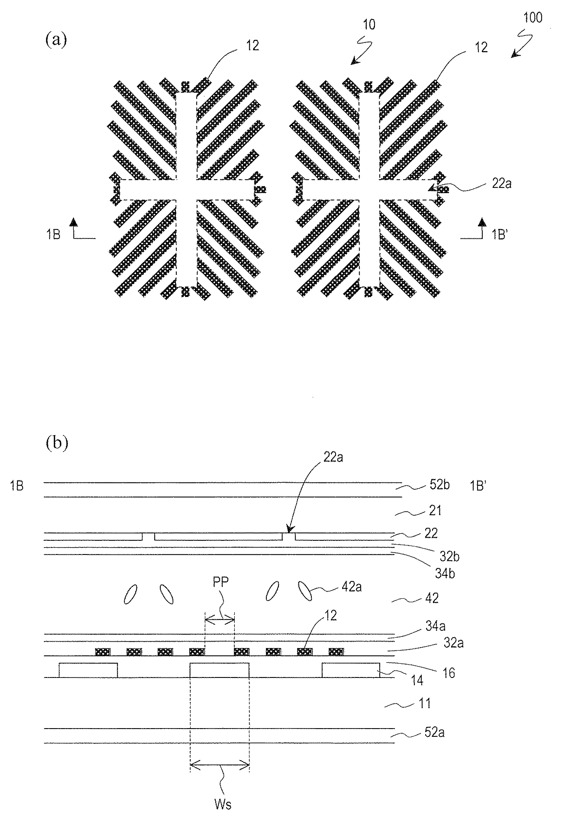
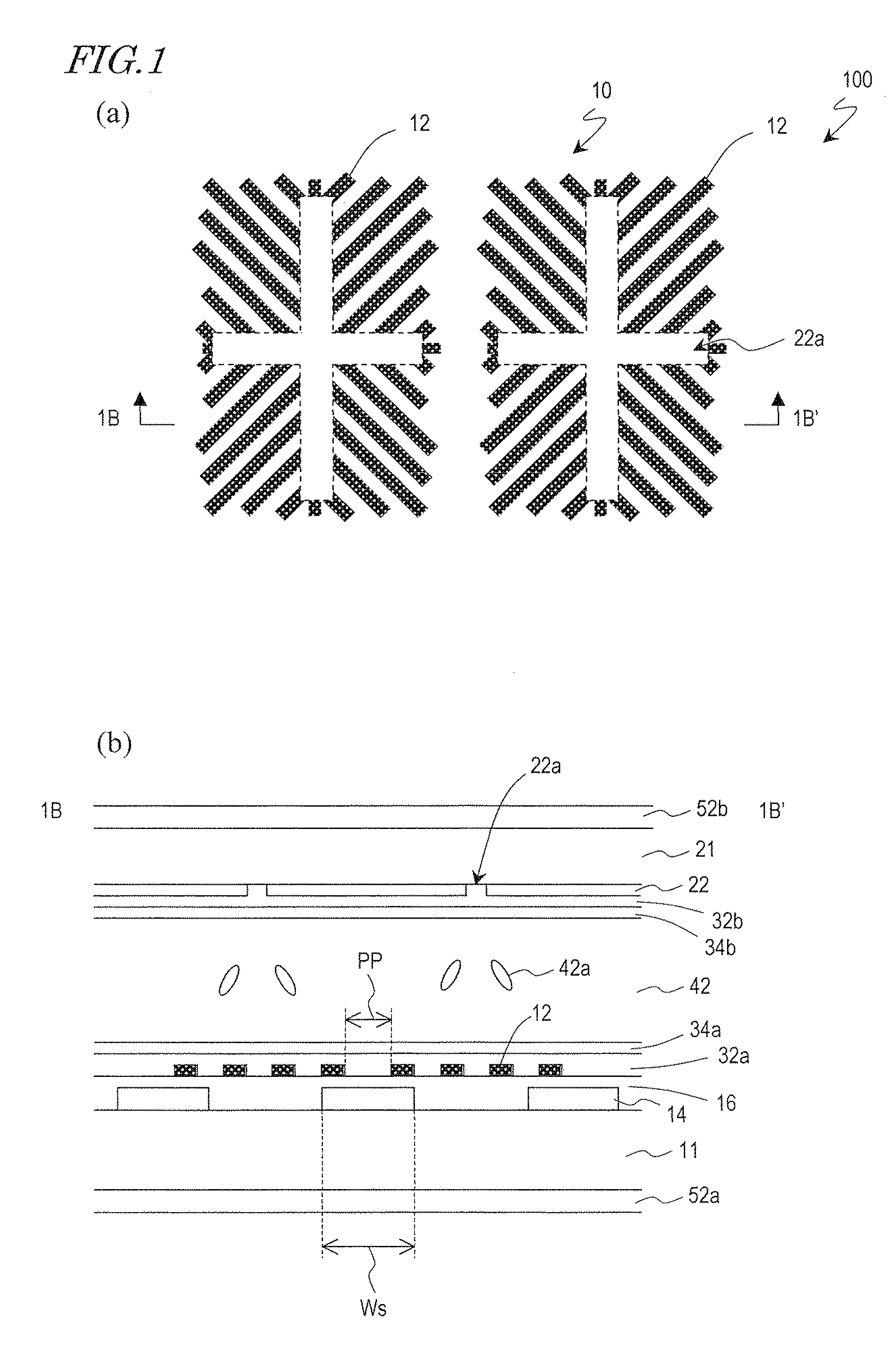
[0059]Hereinafter, a structure and operation of a liquid crystal display device of an embodiment of the present invention are described with reference to the drawings. Note that the present invention is not limited to the embodiment described below.

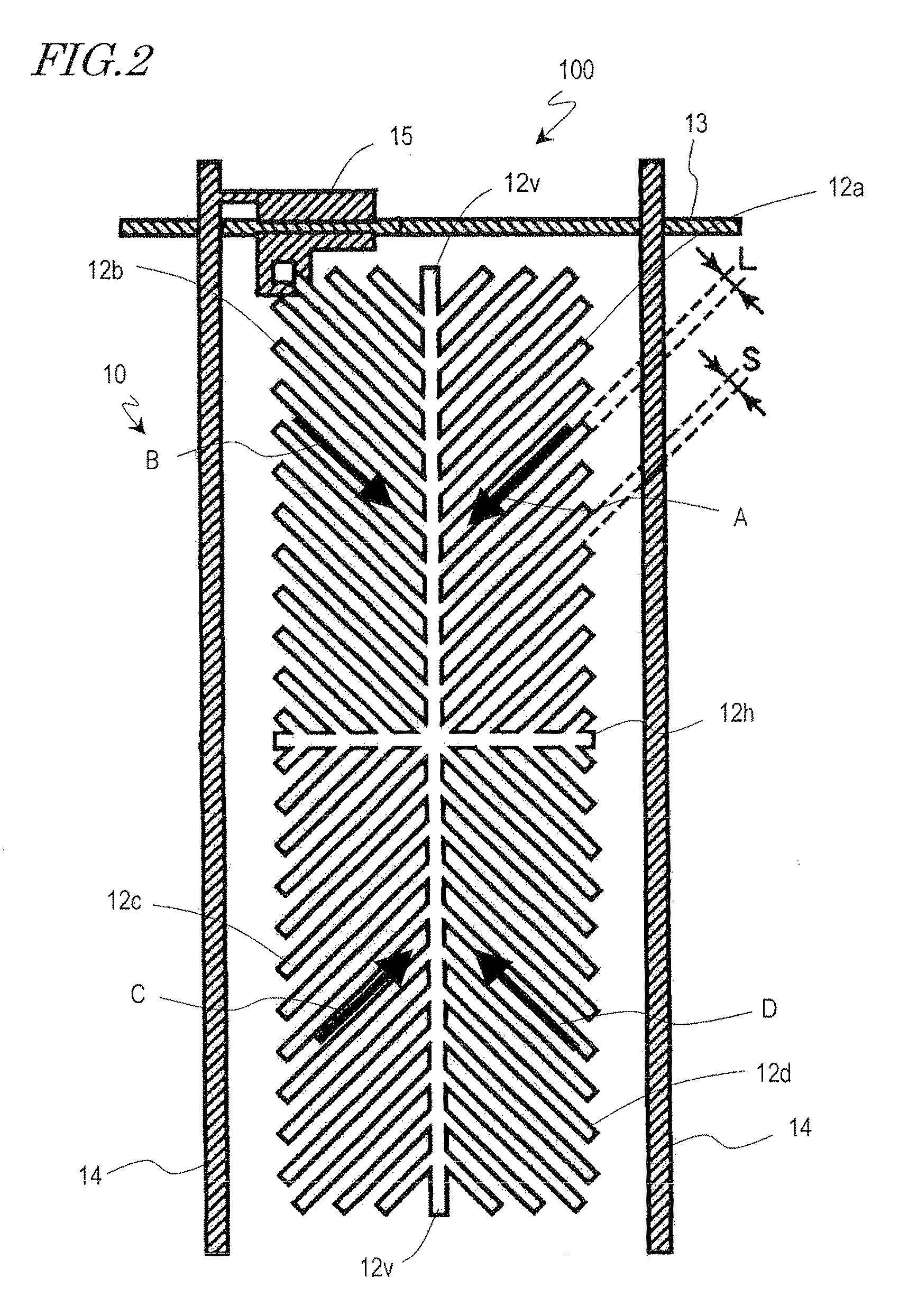
[0060]FIG. 1 schematically shows a structure of two pixels 10 of a liquid crystal display device 100 of an embodiment of the present invention. FIG. 1(a) is a plan view. FIG. 1(b) is a cross-sectional view taken along line 1B-1B′ of FIG. 1(a).

[0061]The liquid crystal display device 100 has a plurality of pixels and includes a pair of substrates 11 and 21 and a pair of polarizing plates 52a and 52b placed in crossed Nicols on the outer sides of the substrates 11 and 21. The liquid crystal display device 100 is configured to display images in a normally black mode. Each pixel has a liquid crystal layer 42 including a nematic liquid crystal material (liquid crystal molecules 42a) whose dielectric anisotropy is negative, and a pixel electrode...


PUM


Abstract

A pixel of a liquid crystal display device of the present invention includes a liquid crystal layer 42, a pixel electrode 12 and a counter electrode 22 opposing each other via the liquid crystal layer, a pair of vertical alignment films 32a, 32b, and alignment sustaining layers 34a, 34b formed by a photopolymerized material on surfaces of the alignment films which are closer to the liquid crystal layer. The pixel electrode has cruciform trunk portions 12h, 12v which are positioned so as to coincide with polarization axes of the pair of polarizing plates and a plurality of branch portions 12a, 12b, 12c, and 12d extending from the cruciform trunk portions in directions of approximately 45°. The counter electrode has a cruciform opening 22a which is positioned so as to oppose the cruciform trunk portions. When a predetermined voltage is applied across the liquid crystal layer, four liquid crystal domains are formed. The pretilt azimuth of a liquid crystal molecule included in a region corresponding to each of the four liquid crystal domains is regulated by the alignment sustaining layers.

Description

TECHNICAL FIELD[0001]The present invention relates to a liquid crystal display device and specifically to an alignment control structure preferably applied to a liquid crystal display device which has a relatively small pixel pitch.[0002]BACKGROUND ART[0003]Recently, as liquid crystal display devices which have wide viewing angle characteristics, transverse electric field mode devices (including IPS mode devices and FFS mode devices) and vertical alignment (VA) mode devices are used. The VA mode devices are superior to the transverse electric field mode devices in terms of mass production and therefore have been used in a wide variety of TV applications and mobile applications.[0004]The VA mode liquid crystal display devices are generally classified into MVA mode devices (see Patent Document 1) and CPA mode devices (see Patent Document 2).[0005]In the MVA mode devices, alignment control means (slit or rib) which has linear portions extending in two directions perpendicular to each o...

Claims


Application Information

Patent Timeline
Patent Type & Authority Applications(United States)
IPC IPC(8): G09G3/36
CPCG02F1/133707G02F1/1393G02F1/134309
Inventor HASHIMOTO, YOSHITOOHGAMI, HIROYUKISHIBASAKI, MASAKAZUKUBO, MASUMISOGA, MASAYUKI
Owner SHARP KK
Why Eureka
Try Eureka