Method of forming monolithic cmos-mems hybrid integrated, packaged structures

Inactive Publication Date: 2011-01-06
AMF NANO
View PDF2 Cites 10 Cited by
  • Summary
  • Abstract
  • Description
  • Claims
  • Application Information

AI Technical Summary

Problems solved by technology

Some of the commonly used micromechanical (MEMS) mechanical structures like polysilicon, nitride etc require high-temperature processing during deposition and annealing to relieve stress and this cannot be performed on the same substrate in the presence of
CMOS electronics due to the lower temperature limitation of the metals in CMOS.
Another limitation of the method is that CMOS requires the substrate to be planar after the MEMS fabrication to achieve high-resolution features in the photolithographic process.
Thus, the current CMOS-MEMS integration methodologies faces serious limitations, requiring sacrificing materials and allowing very little flexibility in device design.
One of the disadvantages with this process is that it needs a dedicated production line and the process is complicated.
The disadvantage of this process is the temperature limitation of the process to below 400° C. to protect the aluminum in the electronics.
Some of the limitations with this process were the warping of the MEMS device due to excessive heating during the laser ablation step.
Som

Method used


Image

  • Method of forming monolithic cmos-mems hybrid integrated, packaged structures
  • Method of forming monolithic cmos-mems hybrid integrated, packaged structures
  • Method of forming monolithic cmos-mems hybrid integrated, packaged structures

Examples


Embodiment Construction

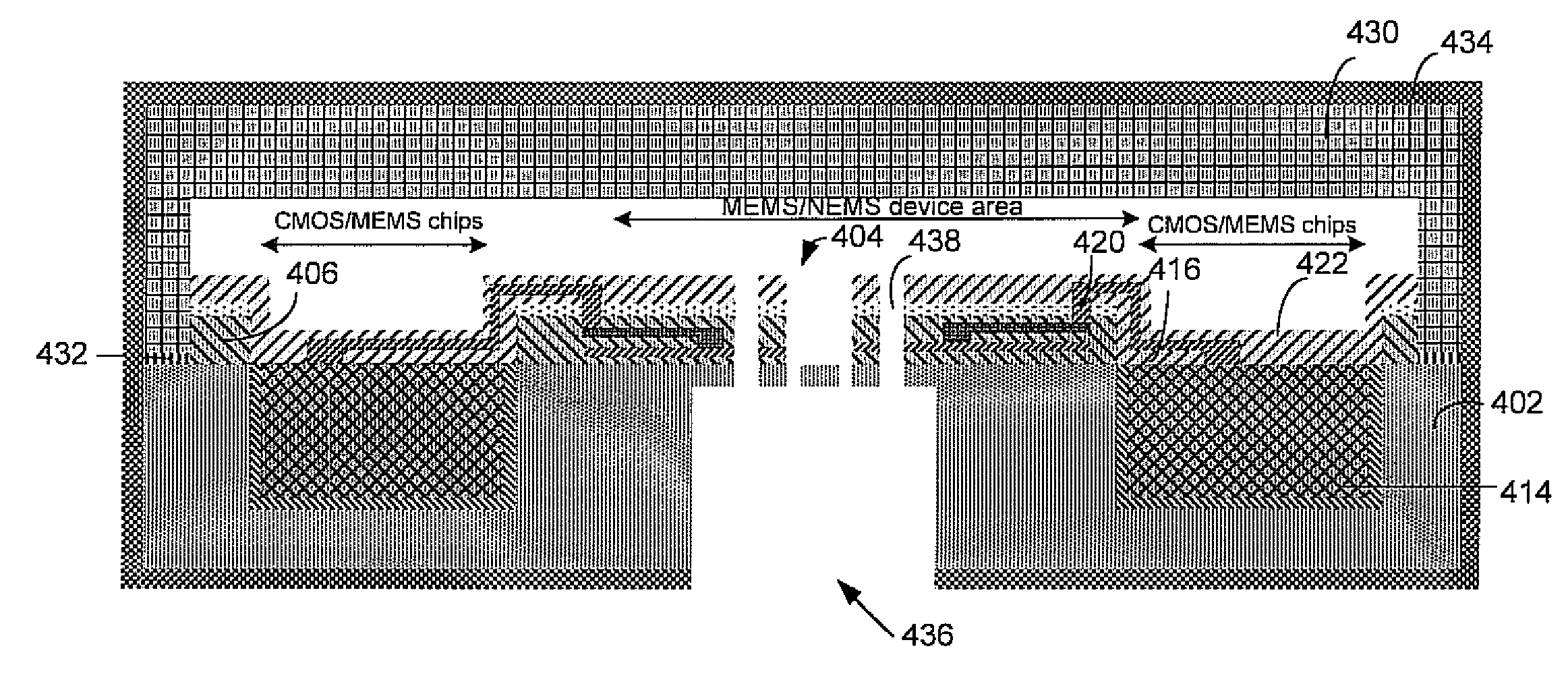
[0028]Referring to the various Figures there is shown an effective, reliable, and relatively low cost method of integration between CMOS-MEMS / NEMS.

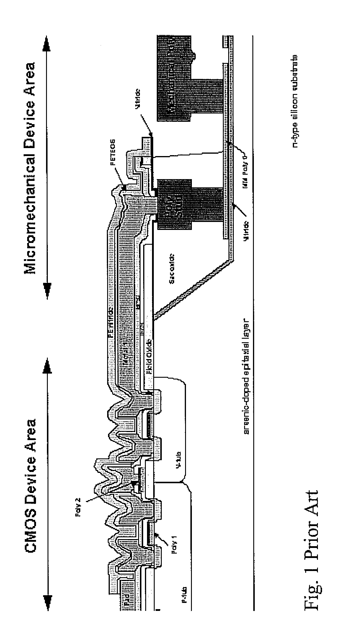
[0029]In one embodiment of a “post CMOS” or “CMOS first” hybrid integration approach shown in FIGS. 3a-3h, the already fabricated CMOS semiconductor substrate is modified to achieve this integration. The CMOS device area is first protected so as not to affect their functionality in the ensuing process; fabrication is continued on the same substrate and integrated by coupling the micromechanical structures in a hybrid approach by placing the MEMS / NEMS dies that have been diced, The integrated system is finally packaged in an effective manner.

[0030]Again referring to FIGS. 3a-h, there is shown a cross-sectional process flow for the “Post CMOS” monolithic hybrid integration approach on a semiconductor substrate 302. A

[0031]CMOS fabricated semiconductor substrate 302 with dielectric layers and metallization in FIG. 3a is provided as a startin...


PUM


Abstract

A method of forming Monolithic CMOS-MEMS hybrid integrated, packaged structures includes the steps of providing: providing at least one semiconductor substrate having a CMOS device area including dielectric layers and metallization layers; applying at least one protective layer overlying the CMOS device area; forming at least one opening on the protective layer and patterning the dielectric and metallization layers to access the semiconductor substrate; forming at least one opening on the semiconductor substrate by etching the dielectric and metallization layers; applying at least one filler layer in the at least one opening on the semiconductor substrate; positioning at least one chip on the filler layer, the chip including a prefabricated front face and a bare backside; applying a first insulating layer covering the front face of the chip providing continuity from the semiconductor substrate to the chip; forming at least one via opening on the insulating layer covering the chip to access at least one contact area; applying at least one metallization layer overlying the insulating layer on the substrate and the chip connecting the metallization layer on the substrate to the at least one another contact area on the chip; applying a second insulating layer overlying the metallization layer on the at least one chip; applying at least one interfacial layer; applying at least one rigid substrate overlying the interfacial layer; and applying at least one secondary protective layer overlying the rigid substrate.

Description

RELATED APPLICATIONS[0001]This application is a continuation-in-part of co-pending U.S. patent application Ser. No. 12 / 497,107 filed Jul. 2, 2009 which is incorporated herein by reference.FIELD OF THE INVENTION[0002]The invention relates to a method for integrating MEMS and CMOS structures.BACKGROUND OF THE INVENTION[0003]Monolithic integration of MEMS / NEMS and electronics offers significant benefits enabling high volume production driving down the per-unit costs of sensor and actuator systems significantly. Micromechanical transducer systems not only need to receive analog and digital electrical inputs and transmit the output, but should also be able to measure rotation, strain, temperature, pressure, acceleration, infrared radiation, micro fluidic chemical properties of liquids and gasses. Effective integration offers other benefits, including, simplifying interconnect issues, reduced packaging and fabrication complexity and significantly improving the overall performance and ease...

Claims


Application Information

Patent Timeline
IPC IPC(8): H01L21/02
CPCB81C1/0023B81C1/00238H01L2924/1461H01L24/24H01L24/82H01L25/0652H01L25/18H01L2224/24227H01L2924/01005H01L2924/01013H01L2924/01015H01L2924/01018H01L2924/01027H01L2924/01029H01L2924/01032H01L2924/01074H01L2924/01077H01L2924/01078H01L2924/01079H01L2924/01082H01L2924/01322H01L2924/09701H01L2924/14H01L2924/16152H01L2924/16235H01L2924/167H01L2924/16788H01L2924/1679H01L2924/19041H01L2924/19042H01L2924/19043H01L2924/01006H01L2924/01033H01L2924/01047H01L2924/014H01L2924/00
Inventor KUMAR, G. KRISHNACHOKSI, NISHIT A.CHALIL, JOSEPH M.
Owner AMF NANO
Why Eureka
Try Eureka