General strength and sensitivity enhancement method for micromachined device

a micromachined device and general strength technology, applied in the direction of microelectromechanical systems, semiconductor devices, semiconductor/solid-state device details, etc., can solve the problems of micromachined structure not being completely achieved, complicated whole process of integrated cmos-mems sensors, and jeopardizing the performance and structure of cmos-mems devices, etc., to achieve the effect of enhancing the performance of micro mention sensors, reducing the displacement of movement, and reducing the displacement of displacemen

Inactive Publication Date: 2011-05-19
HUANG JUNG TANG
View PDF9 Cites 8 Cited by
  • Summary
  • Abstract
  • Description
  • Claims
  • Application Information

AI Technical Summary

Benefits of technology

[0007]The present invention provide a method which employs Electroless plating to deposit extra metal structures on the micromachined structure of CMOS-MEMS micromachined devices. The deposited metal structure can strengthen suspended structures of the original device, and further compensate the residual stress of the suspended structures because it can provide different level of compressive or tensile stress by operating parameters of the plating bath such as temperature, PH value and ingredients.
[0008]Another aspect of this invention is to enhance the performances of micro mention sensors including gyroscopes, accelerometers etc by employing Electroless plating to deposit metal structure on micro structures. Depositing metal structure on the proof mass of the micromachined structure can provide heavier weight, which can increase the displacement of the movement, sensitivity, and can further occupy less proof mass size. Furthermore, Depositing metal structure on the capacitive sensing electrode such as comb-fingers can increase overlap areas of sensing electrode and provide higher capacitive value.

Problems solved by technology

The integrated CMOS-MEMS sensors highly integrate IC processes, MEMS processes and packaging processes, which cause the whole processes of integrated CMOS-MEMS sensors become complicated.
The bottlenecks of current CMOS-MEMS technology include: (a) residual stress, caused by the manufacturing temperature and pressure in thin film process, the characteristics of materials, and film deposition of atomic arrangement, can jeopardize CMOS-MEMS devices' performances and structures.
The current industries still have no better method to conquer residual issues; (b) the standard CMOS process provides fixed recipes including the layer thickness, materials, stacked-layer arrangement and process rules, and devotes highly to the requirements of electronic circuits, rather than micromachined structure design needs; thus, the required recipes of micromachined structure may not be completely achieved by standard semiconductor process; (c) the processes of combining micromachined structure with electronic circuits in one chip are complex and difficult, which increase the total costs; (d) mechanical properties can not be reached.
Because of consideration for stability, yield rate and price, the current semiconductor process may not achieve certain requirements of CMOS-MEMS micro-machined devices.
Domestic and foreign scholars, and some international companies have brought up the following methods to increase sensitivity of MEMS motion sensors; (a) using Silicon On Insulation (SOC) wafer to be structural substrate, but high cost; (b) employing electroforming to increase the weight of proof mess, which is difficult to control the quality, height and uniformity of electroformed films, and damages the performance of circuits; (c) employing sputtering technology to deposit extra film to gain the weight of proof mess, but low deposition rate and not cost-effective; (d) utilizing etching technology such as dry and wet etching to form bulk machining, but complicated process and high cost.

Method used


Image

  • General strength and sensitivity enhancement method for micromachined device
  • General strength and sensitivity enhancement method for micromachined device
  • General strength and sensitivity enhancement method for micromachined device

Examples


embodiment 1

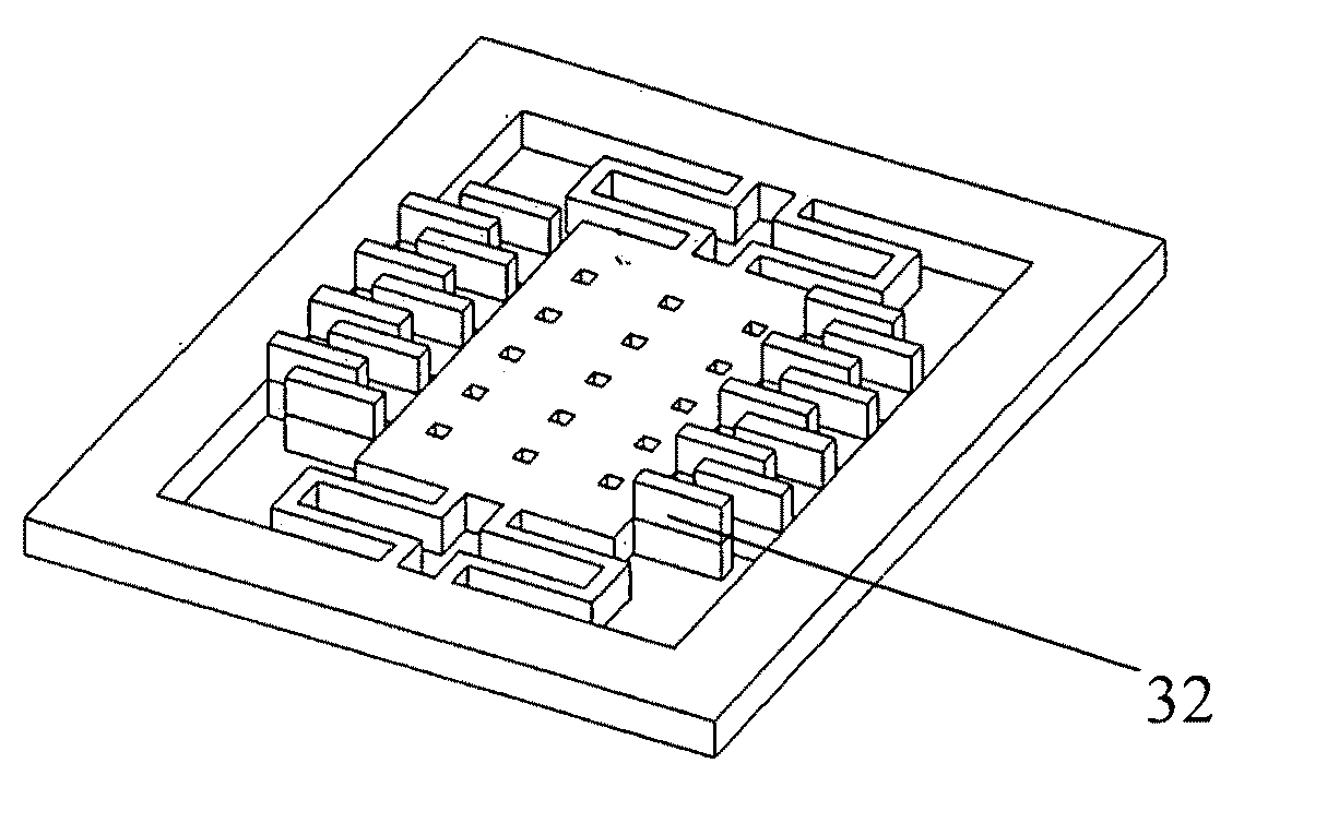
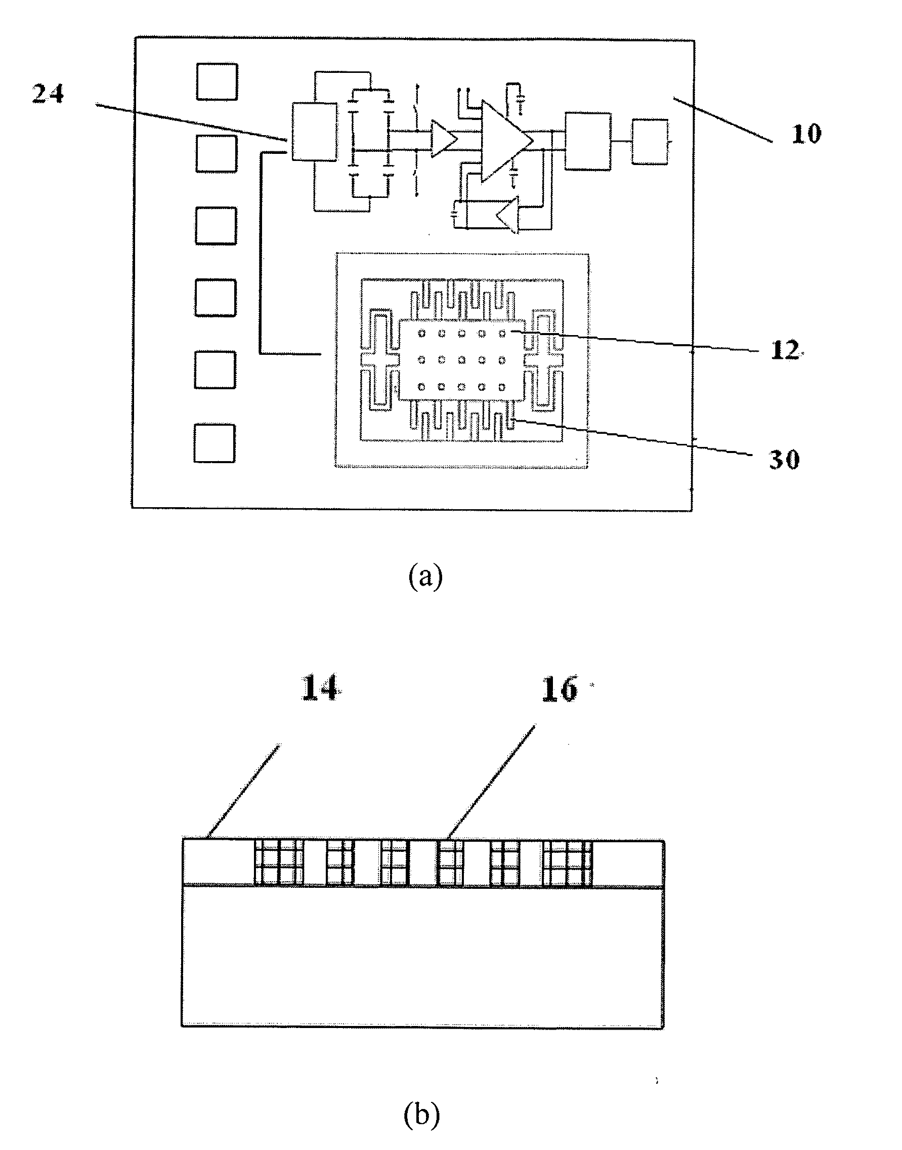
[0018]Referring to FIG. 1, it illustrates the schematic process flow for increasing the weight of proof mass 12, enhancing the sensitivity, strengthening the micro structures, minimizing the size, and compensating suspended micromachined structure for residual stress, which can apply to CMOS-MEMS devices 10 such as accelerometer, gyroscope, micro motion sensors, etc. The process of this embodiment comprises the following steps of:

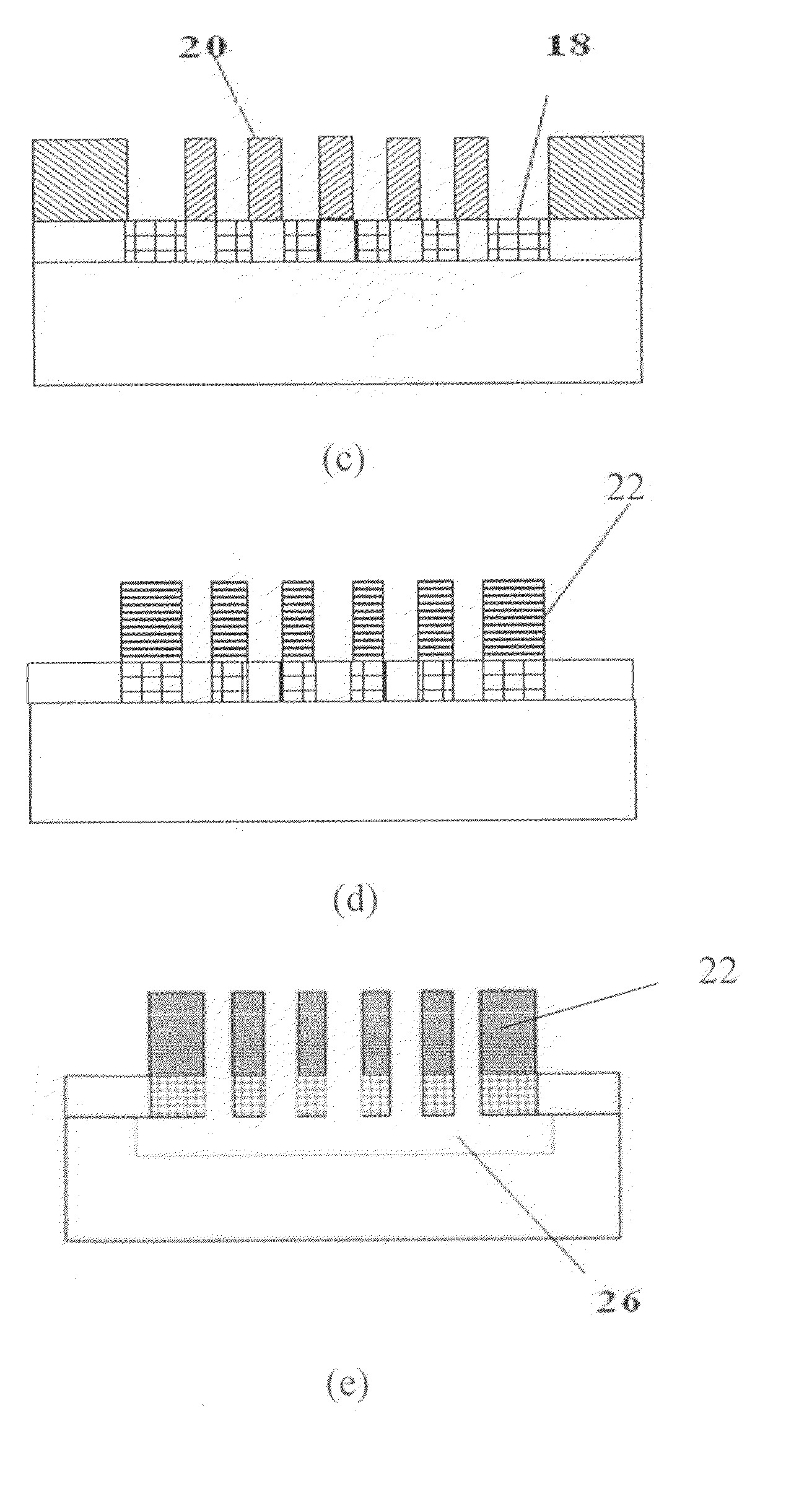
[0019]Step 1, designing CMOS-MEMS devices and defining the deposited region for deposited metal structure. Employ standard semiconductor process such as 0.35 μm CMOS processes to produce CMOS-MEMS device 10 which contains micromachined structures, proof mass, comb-finger structures and the deposited regions on the proof mass of micromachined structures by the top metal layer 16 and passivation layer 14, shown as FIG. 1(b). Further, CMOS-MEMS devices 10 can contain amplifier, drivers and measuring circuits 24.

[0020]Step 2, patterning cavities through photoli...


PUM

PropertyMeasurementUnit
temperatureaaaaaaaaaa
thicknessaaaaaaaaaa
thicknessaaaaaaaaaa

Abstract

This invention disclosed a method to strengthen structure and enhance sensitivity for CMOS-MEMS micro-machined devices which include micro-motion sensor, micro-actuator and RF switch. The steps of the said method contain defining deposited region by metal and passivation layer, forming a cavity for depositing metal structure by lithography process, depositing metal structure on the top metal layer of micromachined structure by Electroless plating, polishing process and etching process. The method aims at strengthening structures and minimizing CMOS-MEMS device size. Furthermore, this method can also be applied to inertia sensors such as accelerometer or gyroscope, which can enhance sensitivity and capacitive value, and deal with curl issues for suspended CMOS-MEMS devices.

Description

FIELD OF INVENTION[0001]This invention disclosed a method to strengthen structure and enhance sensitivity for CMOS-MEMS micro-machined devices which include micro motion sensor, micro actuator and RF switch. The steps of the said method contain defining the deposited region by metal layer and passivation layer, forming a PR cavity for depositing metal structure by lithography process, depositing metal structure on the top metal layer of micromachined structure by Electroless plating, polishing process and etching process. The method aims at strengthening structures and minimizing CMOS-MEMS device size. Furthermore, this method can also be applied to motion sensors such as accelerometer or gyroscope, which can enhance sensitivity and capacitive value, and deal with curl issues for suspended CMOS-MEMS devices.DESCRIPTION OF RELATED ART[0002]System on chip (SOC) technology has gradually accommodated CMOS-MEMS products such as micro sensors, micro actuators or micro structures, which as...

Claims


Application Information

Patent Timeline
Patent Type & Authority Applications(United States)
IPC IPC(8): H01L23/14H01L21/445
CPCB81B3/0086B81B2201/0235B81B2201/0242B81C2203/0714B81B2207/015B81C2201/0167B81C2201/0197B81B2203/0136
Inventor HUANG, JUNG-TANGLIN, MING-JHEHSU, HOU-JUN
Owner HUANG JUNG TANG
Why Eureka
Try Eureka