

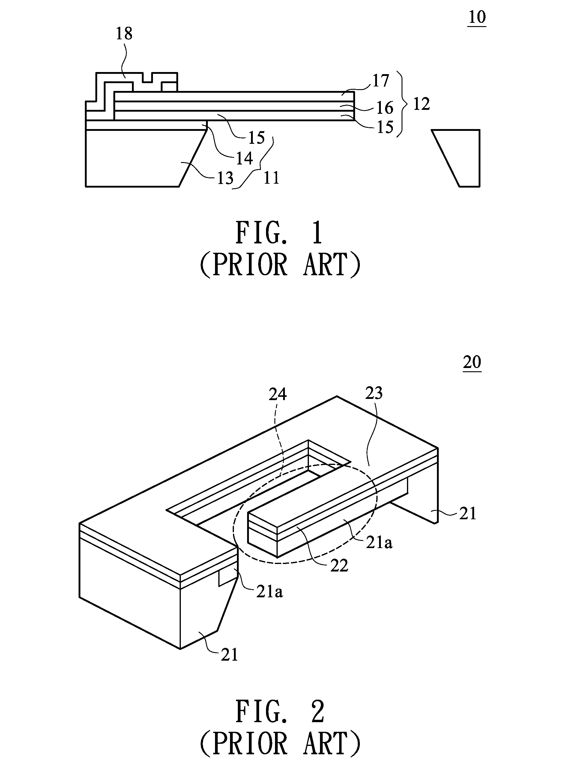
CMOS-MEMS Cantilever Structure
a technology of cantilever beams and cantilever beams, applied in the direction of microstructural systems, microstructure devices, volume/mass flow by dynamic fluid flow effect, etc., can solve the problems of increased cost, inability to meet the needs of the application, and the cantilever beams described above suffer from shortcomings in practical application, so as to improve the sensing sensitivity of the cantilever beam, reduce manufacturing costs, and simplify the manufacturing process
- Summary
- Abstract
- Description
- Claims
- Application Information
AI Technical Summary
Benefits of technology
Problems solved by technology
Method used
Image

Examples
Embodiment Construction
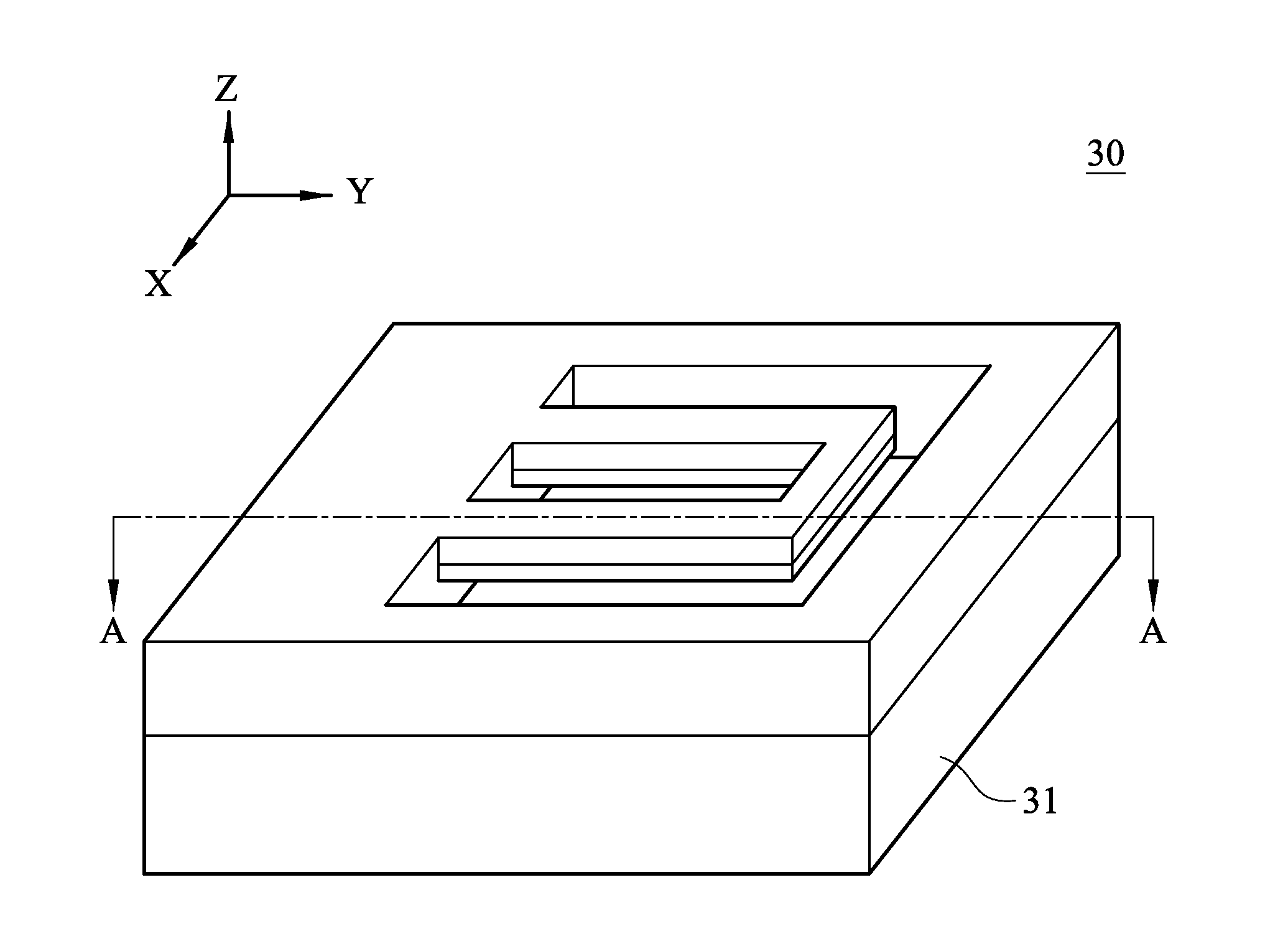
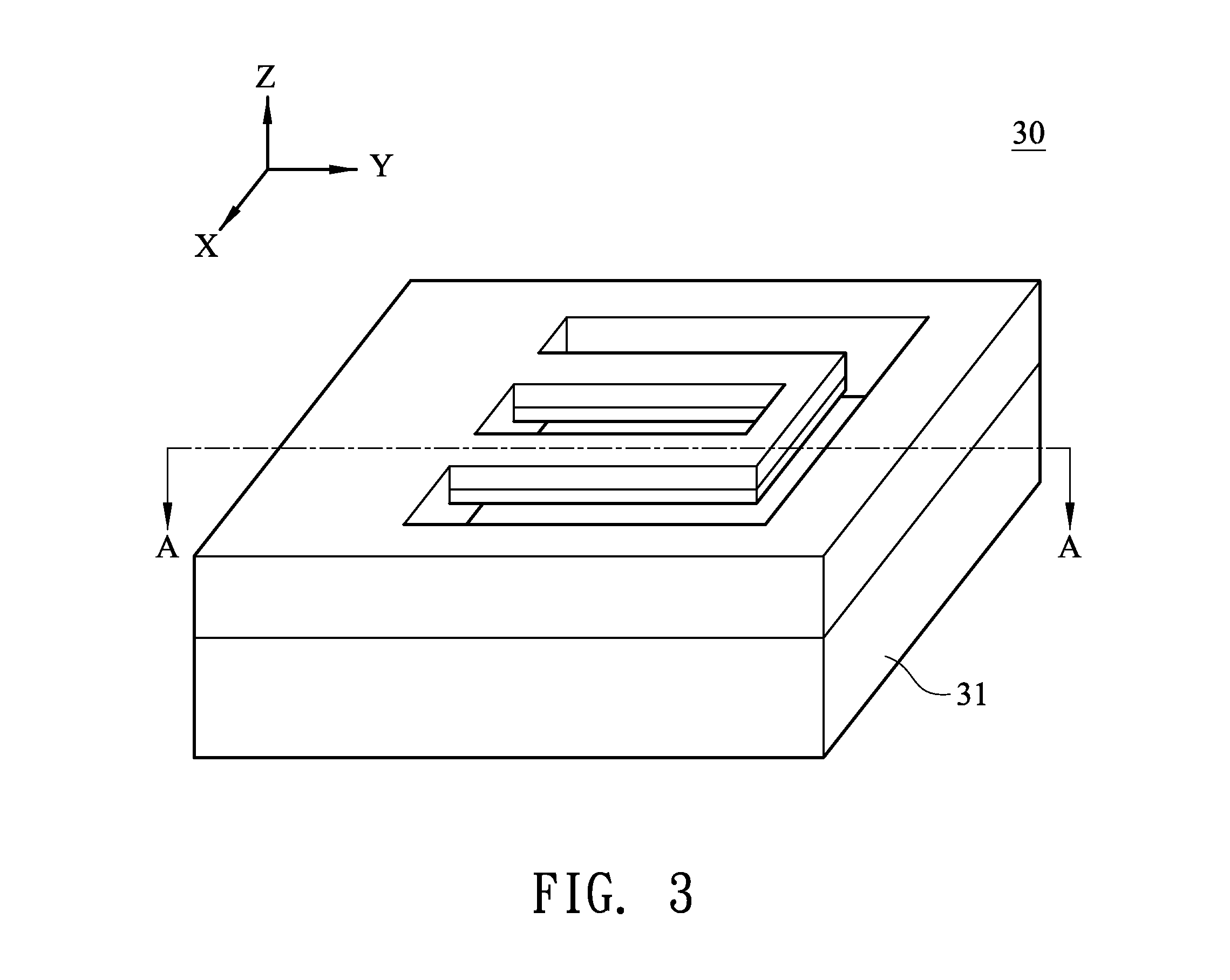
[0020]Referring to both FIG. 3 and FIG. 4, according to an embodiment of the present invention, a CMOS-MEMS cantilever structure 30 includes a substrate 31, a circuit structure 34 and a cantilever beam 35. The substrate 31 is a silicon substrate having a circuit area 32 and a sensor unit area 33 defined thereon. Moreover, the substrate 31 further has a depressed area 41 in the sensor unit area 33, depressed inwards from the surface of the substrate 31. On the substrate 31 are formed a circuit structure 34 and a cantilever beam 35, respectively formed in the circuit area 32 and the sensor unit area 33. The circuit structure 34 and the cantilever beam 35 are both fabricated by deposition in a CMOS standard manufacturing process.
[0021]The circuit structure 34 includes a first oxide layer 38, a polysilicon layer 36 and a second oxide layer 39, wherein the first oxide layer 38 is formed by silicon dioxide which is mainly used in forming the gate oxide layer of a transistor and therefore ...
PUM
 Abstract
Description
Claims
Application Information