Semiconductor device

a technology of semiconductor devices and semiconductors, applied in the direction of semiconductor devices, basic electric elements, electrical appliances, etc., can solve the problems of increasing the variation in the value of current b>9/b>, i.e., the size reduction, etc., and achieve excellent effect, increase the sense ratio, and reduce the variation in the current value at which the overcurrent protection operates

Active Publication Date: 2011-01-13
PANASONIC SEMICON SOLUTIONS CO LTD
View PDF5 Cites 0 Cited by
  • Summary
  • Abstract
  • Description
  • Claims
  • Application Information

AI Technical Summary

Benefits of technology

[0018]In the first inventive semiconductor device, the second emitter region, which is electrically connected with the current detection means and is electrically connected with the first emitter region through the detection resistor (a sense resistor) in the current detection means, is formed in the high-voltage semiconductor switching element, i.e., in a lateral IGBT, in addition to the emitter region (the first emitter region) that is necessary for switching operations. Also, the emitter electrode is not formed on the second emitter region, while the emitter electrode is formed on a part of the base region that is adjacent to the second emitter region. It is thus possible to prevent a hole current of the current passing through the lateral IGBT from flowing from the second emitter region to the sense resistor. In other words, only an electron current passing through the second emitter region flows to the sense resistor. Hence, the current (a sense current) passing through the sense resistor can be reduced without designing the sense resistor with a small resistance value and the second emitter region of a small size. Thus, in the first inventive semiconductor device having the overcurrent protection function for the high-voltage semiconductor switching element, the ratio between the current flowing from the second emitter region to the sense resistor and the current flowing through the high-voltage semiconductor switching element, that is, a sense ratio, can be made twice as much or higher than that obtained in the conventional semiconductor device. As a result, the resistance value of the sense resistor and the size of the second emitter region can be designed to be larger, so that variations in the current value at which the overcurrent protection operates can be reduced.
[0030]As set forth above, the invention relates to a semiconductor device including an insulated gate switching element. More particularly, when applied to a semiconductor device that includes an overcurrent protection circuit to protect a switching element from an overcurrent, the invention produces an excellent effect, in which variations in a current value at which the overcurrent protection operates are reduced by increasing the ratio between a current flowing through a sense resistor and a current flowing through the high-voltage semiconductor switching element, and is thus very beneficial.

Problems solved by technology

However, the conventional semiconductor device having the overcurrent protection function for the lateral IGBT has a following problem described below.
In this case, however, the problem of increased variation in the value of the current 9, i.e., in the current value at which the overcurrent protection function operates, caused by the reduction in the size of the lateral IGBT 2, is again unavoidable.

Method used


Image

  • Semiconductor device
  • Semiconductor device
  • Semiconductor device

Examples


first embodiment

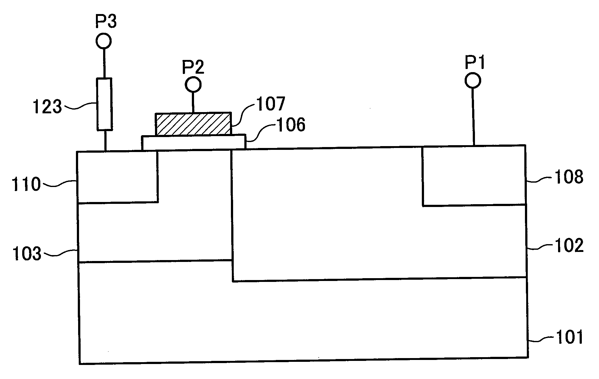
[0045]A semiconductor device, specifically, a semiconductor device having a high-voltage semiconductor switching element and an overcurrent protection function for the element, according to a first embodiment of the invention will be described with reference to the accompanying drawings.

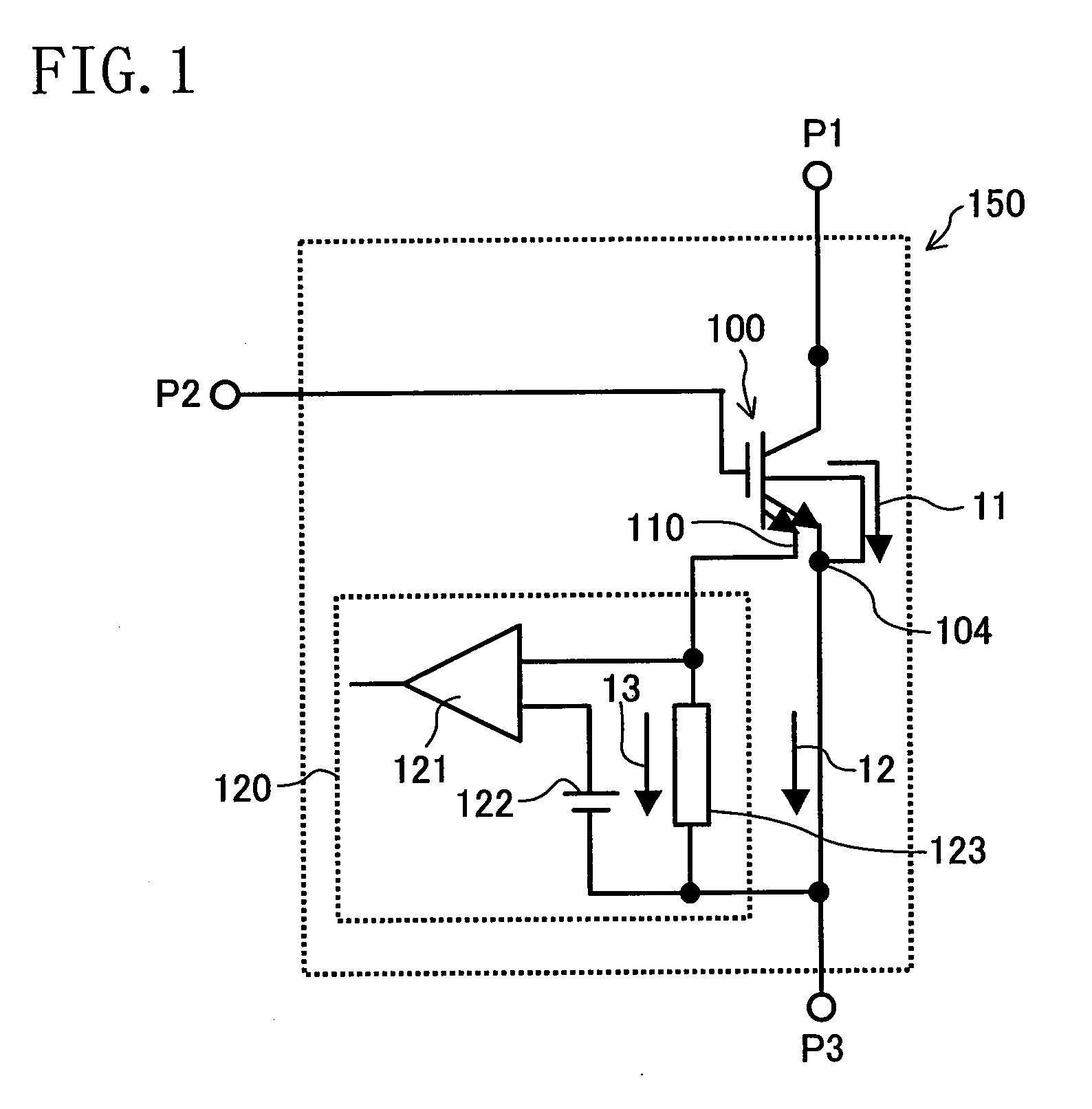
[0046]FIG. 1 shows the rough circuit configuration of the semiconductor device of this embodiment. As shown in FIG. 1, the semiconductor device 150 of this embodiment includes a high-voltage semiconductor switching element 100 composed of a lateral IGBT controlled by a gate voltage applied to a gate electrode. A collector region in the high-voltage semiconductor switching element 100 is electrically connected to a collector terminal (a collector electrode) P1, while a gate electrode of the high-voltage semiconductor switching element 100 is electrically connected with a gate terminal P2. As a characteristic of the semiconductor device of this embodiment, a part (hereinafter referred to as a “second e...

second embodiment

[0063]A semiconductor device, specifically, a semiconductor device having a high-voltage semiconductor switching element and an overcurrent protection function for the element, according to a second embodiment of the invention will be described with reference to the accompanying drawings. The rough circuit configuration of the semiconductor device of this embodiment is the same as that of the first embodiment shown in FIG. 1, and duplicated descriptions will be thus omitted herein. However, in this embodiment, the first emitter region 104 should be read as a first emitter / source region 104, the second emitter region 110 as a second emitter / source region 110, the collector terminal P1 as a collector / drain terminal (a collector / drain electrode) P1, and the emitter terminal P3 as an emitter / source terminal (an emitter / source electrode) P3.

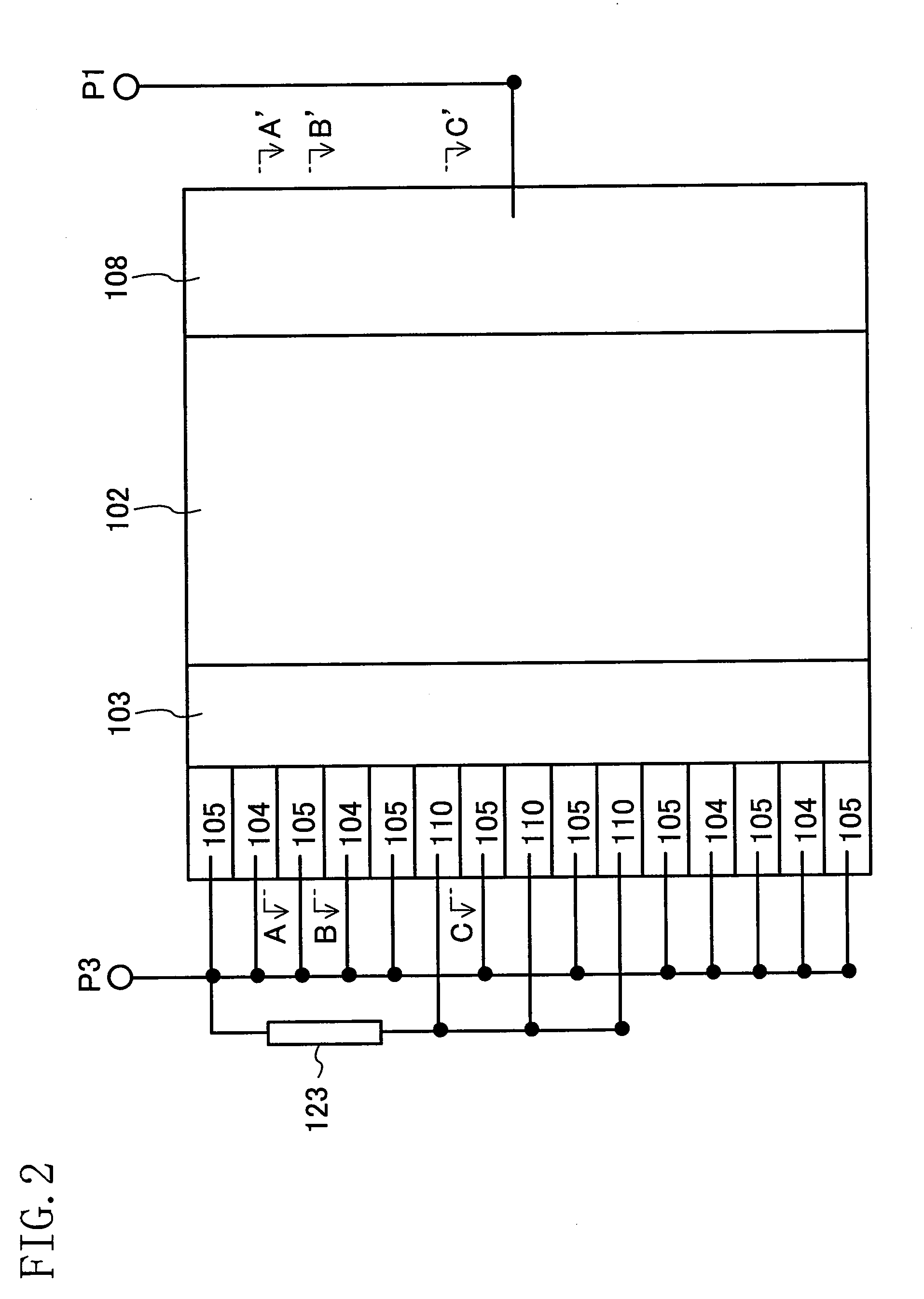
[0064]FIG. 6 is a plan view of the high-voltage semiconductor switching element 100 in the semiconductor device 150 of FIG. 1 according to this embod...

third embodiment

[0077]A semiconductor device, specifically, a semiconductor device having a high-voltage semiconductor switching element and an overcurrent protection function for the element, according to a third embodiment of the invention will be described with reference to the accompanying drawings. The rough circuit configuration of the semiconductor device of this embodiment is the same as that of the first embodiment shown in FIG. 1, and duplicated descriptions will be thus omitted herein. However, in this embodiment, the first emitter region 104 should be read as a first emitter / source region 104, the second emitter region 110 as a second emitter / source region 110, the collector terminal P1 as a collector / drain terminal (a collector / drain electrode) P1, and the emitter terminal P3 as an emitter / source terminal (an emitter / source electrode) P3.

[0078]FIG. 10 is a plan view of the high-voltage semiconductor switching element 100 in the semiconductor device 150 of FIG. 1 according to this embod...


PUM


Abstract

In a high-voltage semiconductor switching element, in addition to a first emitter region that is necessary for switching operations, a second emitter region, which is electrically connected with the first emitter region through a detection resistor in current detection means and is electrically connected with the current detection means, is formed. No emitter electrode is formed on the second emitter region, while an emitter electrode is formed on a part of a base region that is adjacent to the second emitter region.

Description

BACKGROUND OF THE INVENTION[0001]1. Field of the Invention[0002]The present invention relates to a semiconductor device including an insulated gate switching element, and more particularly relates to a semiconductor device including an overcurrent protection circuit to protect a switching element from an overcurrent.[0003]2. Description of the Related Art[0004]FIG. 12 shows a typical cross-sectional configuration of a lateral insulated gate bipolar transistor (hereinafter referred to as an “IGBT”) which is used as a high-voltage semiconductor switching element. As shown in FIG. 12, an N-type extended drain region 52 and a P-type base region 53 adjacent to the extended drain region 52 are formed in surface portions of a semiconductor substrate 51. An N+-type emitter region 54 is formed in a surface portion of the base region 53 so as to be spaced apart from the extended drain region 52. A gate insulating film 56 is formed on the base region 53 so as to extend on a part of the emitter...

Claims


Application Information

Patent Timeline
Patent Type & Authority Applications(United States)
IPC IPC(8): H01L29/739
CPCH01L29/7393
Inventor YAMAGIWA, HIROTOSAJI, TAKASHIKANEKO, SAICHIRO
Owner PANASONIC SEMICON SOLUTIONS CO LTD
Why Eureka
Try Eureka