Thin touch panel

a touch panel and touch technology, applied in the field of thin touch panel, can solve the problems of increasing the total height of the capacitive touch module, increasing consuming more materials during manufacturing, so as to reduce the cost of the sticking process, increase the transparency of the touch panel, and reduce the material consumption

Active Publication Date: 2011-01-13
BUWON PRECISION SCI
View PDF1 Cites 40 Cited by
  • Summary
  • Abstract
  • Description
  • Claims
  • Application Information

AI Technical Summary

Benefits of technology

[0004]The present invention is directed to a thin touch panel, wherein a black bordering, a transparent sensing layer, a plurality of metal connecting structures, a plurality of metal guiding lines and a plurality of transparent insulators are formed on an inner surface of a transparent substrate directly. Thus, the transparent substrate may not only be a touch end, but also have a touch control ability of thin touch panel directly. Comparing to the conventional touch panel, the glass substrate of the touch panel disposed between the cover lens and the display panel may be simplified, so as to reduce material consumption and increase a transparency of the touch panel. In addition, the process of sticking the cover lens and the glass substrate by using the optical adhesive may be left out, so as to further reduce the cost of the sticking process and enhance the yield rate. Furthermore, the thickness of the whole structure of the touch panel is reduced, so as to benefit a design tendency of thinning out the product.

Problems solved by technology

Thus, more materials may be consumed during manufacturing.
However, the assembling process not only more complicated and spends much time, but also increases the total height of the capacitive touch module 12, thus unable to confirm lighter and thinner requirement of the existing electronic products.
Furthermore, since the optical adhesive 22 is much expensive and hard to be stuck well, all the optical adhesive 22, the capacitive touch panel 16 and cover lens 18 have to be discarded because of unable to be reworked.
Thus, these materials are wasted.

Method used


Image

  • Thin touch panel
  • Thin touch panel
  • Thin touch panel

Examples


Embodiment Construction

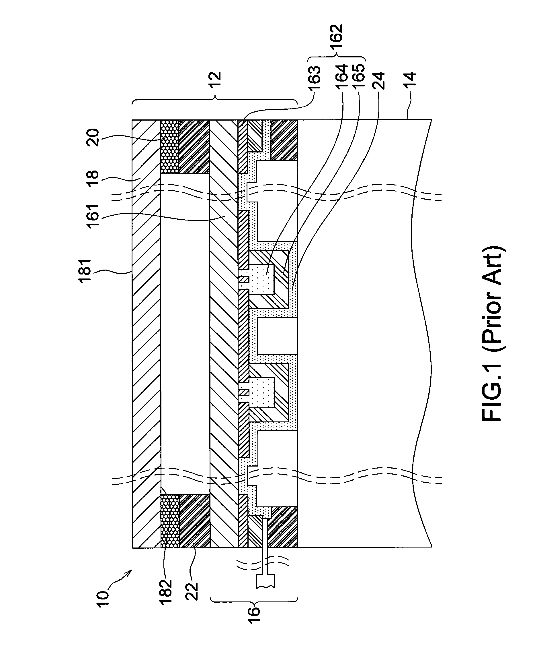
[0022]Reference will now be made in detail to specific embodiments of the present invention. Examples of these embodiments are illustrated in the accompanying drawings. While the invention will be described in conjunction with these specific embodiments, it will be understood that it is not intended to limit the invention to these embodiments. In fact, it is intended to cover alternatives, modifications, and equivalents as may be included within the spirit and scope of the invention as defined by the appended claims. In the following description, numerous specific details are set forth in order to provide a through understanding of the present invention. The present invention may be practiced without some or all of these specific details. In other instances, well-known process operations are not described in detail in order not to obscure the present invention.

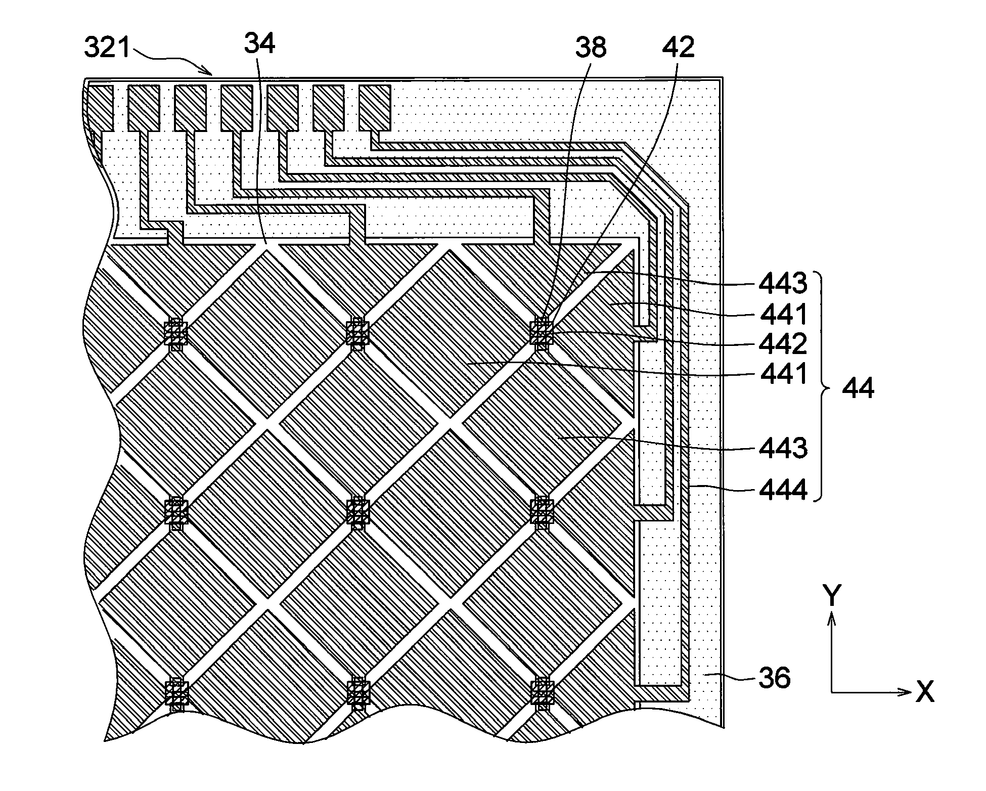
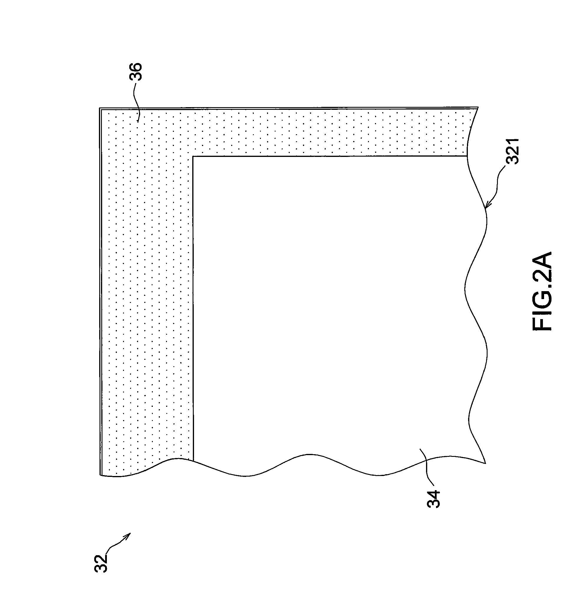
[0023]Referring to FIG. 2A, a thin touch panel comprises a transparent substrate 32 having an outer surface (not shown) and ...


PUM

PropertyMeasurementUnit
transparentaaaaaaaaaa
transparent conductiveaaaaaaaaaa
total heightaaaaaaaaaa

Abstract

A thin touch panel includes a transparent substrate with a black bordering around the inner surface of the transparent substrate. A plurality of metal connecting structures, metal guiding lines, transparent insulating structures and a transparent sensing layer are formed on the inner surface, so that the transparent substrate not only provides a touch surface, but also has the touch sensing ability, to decrease the manufacture material and increase the transmittance of the touch panel. Besides, the manufacture of the thin touch panel may not use any optical adhesive to decrease the manufacture cost and improve the yield. Further, the thin touch panel may satisfy the trend of thin design.

Description

FIELD OF THE INVENTION[0001]The present invention generally relates to a capacitive touch panel, and more particularly to a thin touch panel.DESCRIPTION OF THE RELATED ART[0002]Most of the existing electronic products such as handheld computer, personal digital assistant (PDA), and information appliance (IA) may be equipped with a touch display screen 10 as illustrated in FIG. 1. The touch display screen 10 mainly comprises a capacitive touch module 12 and a display panel 14. The conventional capacitive touch module 12 comprises a capacitive touch panel 16 and a cover lens 18. A top surface 181 of the cover lens 18 is capable of being a finger touch region. A black pattern 20 is formed on edges of a bottom surface 182 of the cover lens 18, and the black pattern 20 is tightly combined with a glass substrate 161 of the capacitive touch panel 16 by sticking an optical adhesive 22. A sensing circuit layer 162 consisted of a transparent conductive film 163 such as indium tin oxide (ITO),...

Claims


Application Information

Patent Timeline
Patent Type & Authority Applications(United States)
IPC IPC(8): G06F3/041
CPCG06F3/041G06F3/047
Inventor LEE, SHENG-FENGWEN, CHING-HSIEN
Owner BUWON PRECISION SCI
Why Eureka
Try Eureka