Method of forming a group iii-nitride crystalline film on a patterned substrate by hydride vapor phase epitaxy (HVPE)

a technology of hydride vapor phase and crystalline film, which is applied in the direction of coating, chemical vapor deposition coating, semiconductor devices, etc., can solve the problems of limited use of group iii-nitrides in many applications and not providing the highest crystalline quality films, and achieves low defect and high quality

Active Publication Date: 2011-01-20
APPLIED MATERIALS INC
View PDF50 Cites 89 Cited by
  • Summary
  • Abstract
  • Description
  • Claims
  • Application Information

AI Technical Summary

Benefits of technology

[0007]A method of depositing a high quality low defect single crystalline Group III-Nitride film. A patterned substrate having a plurality of features with inclined sidewalls separated by spaces is provided. A Group III-Nitride film is deposited by a hydride vapor phase epitaxy (HVPE) process over the patterned substrate. The HVPE deposition process forms a Group I...

Problems solved by technology

The use of Group III-Nitrides in many applications has been limited by very high dislocation densities usually in the...

Method used


Image

  • Method of forming a group iii-nitride crystalline film on a patterned substrate by hydride vapor phase epitaxy (HVPE)
  • Method of forming a group iii-nitride crystalline film on a patterned substrate by hydride vapor phase epitaxy (HVPE)
  • Method of forming a group iii-nitride crystalline film on a patterned substrate by hydride vapor phase epitaxy (HVPE)

Examples


Embodiment Construction

[0028]Embodiments of the present invention include a method of forming a high quality low defect density Group III-Nitride film on a patterned substrate. The present invention has been described with respect to specific details in order to provide a thorough understanding of the invention. One of ordinary skill in the art will appreciate that the invention can be practiced without these specific details. In other instances, will known semiconductor processes and equipment have not been described in specific detail in order to not unnecessarily obscure the present invention.

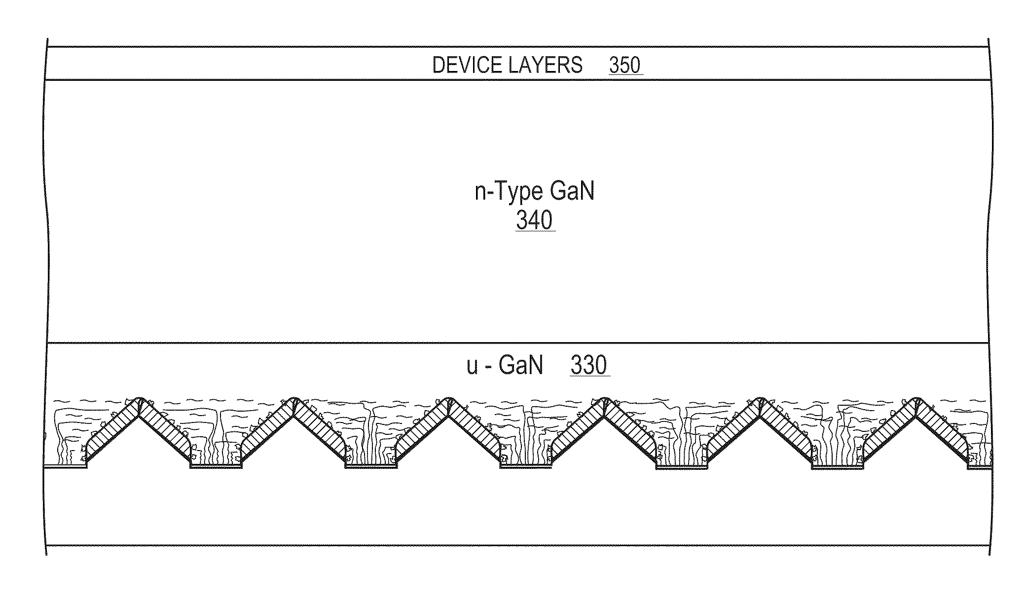
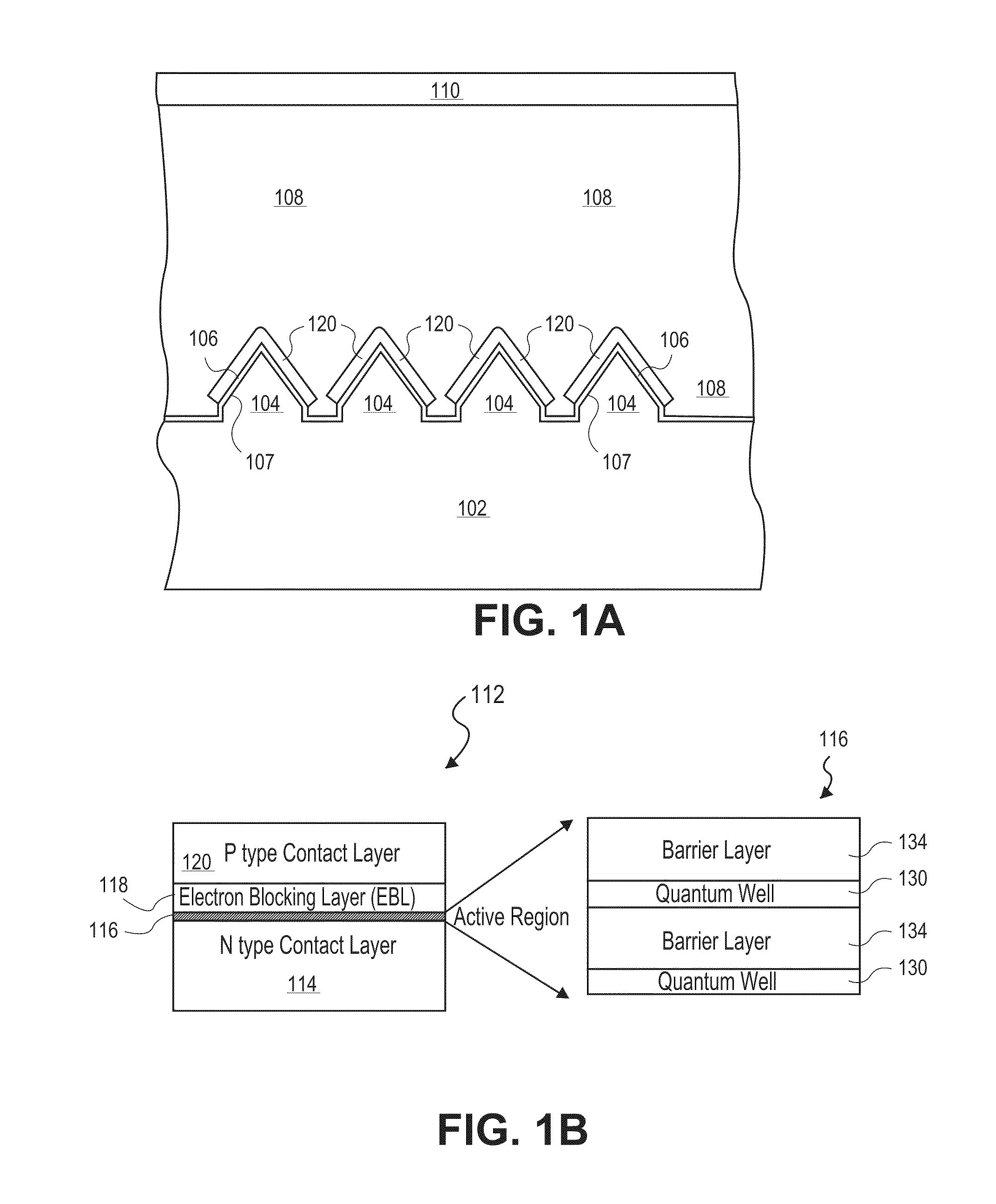
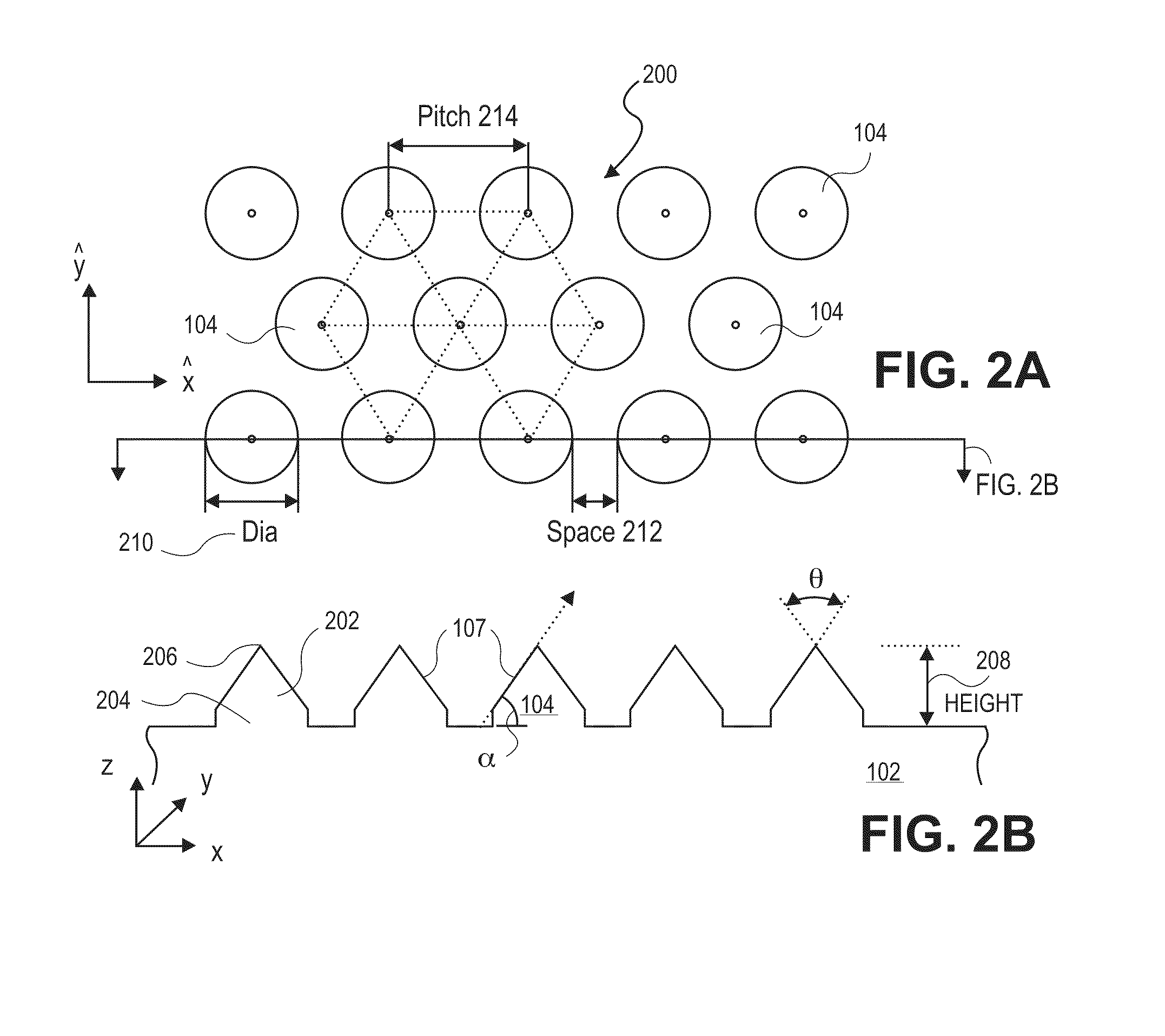
[0029]The present invention is a method of forming a high quality, low defect density Group III-Nitride crystalline film. According to embodiments of the present invention, a Group III-Nitride crystalline semiconductor film is formed by a hydride vapor phase epitaxial (HVPE) deposition process onto a patterned substrate. Embodiments of the present invention utilize substrate features of a desired shape, spacing, h...


PUM

PropertyMeasurementUnit
Thicknessaaaaaaaaaa
Angleaaaaaaaaaa
Temperatureaaaaaaaaaa

Abstract

A method of depositing a high quality low defect single crystalline Group III-Nitride film. A patterned substrate having a plurality of features with inclined sidewalls separated by spaces is provided. A Group III-Nitride film is deposited by a hydride vapor phase epitaxy (HVPE) process over the patterned substrate. The HVPE deposition process forms a Group III-Nitride film having a first crystal orientation in the spaces between features and a second different crystal orientation on the inclined sidewalls. The first crystal orientation in the spaces subsequently overgrows the second crystal orientation on the sidewalls and in the process turns over and terminates treading dislocations formed in the first crystal orientation.

Description

[0001]This Application claims the benefit of and priority to Provisional Application Ser. No. 61 / 226,440 filed Jul. 17, 2009 which is hereby incorporated by reference.BACKGROUND[0002]1. Field[0003]Embodiments of the present invention describe a method a manufacturing a high quality low dislocation density Group III-Nitride layer at a high growth rate by HVPE on a patterned substrate.[0004]2. Discussion of Related Art[0005]Group III-Nitride semiconductors are finding greater importance in the development and fabrication of the variety of semiconductor devices, such as light emitting diodes (LEDs), laser diodes (LDs) and electronic devices, such as high electron mobility transistors (HEMTs), hetero junction bipolar transistors (HBTs). An important requirement in forming these semiconductor devices is the fabrication of a suitably thick Group III-Nitride layer, such as a gallium nitride layer (GaN), with a smooth surface and a low dislocation density.[0006]Presently Group III-Nitride l...

Claims


Application Information

Patent Timeline
IPC IPC(8): H01L29/66H01L21/20
CPCH01L21/0237H01L29/04H01L21/0243H01L21/02433H01L21/02439H01L21/02458H01L21/02488H01L21/0254H01L21/0262H01L21/02639H01L21/02647H01L33/007H01L33/12H01L33/16H01L33/22H01L21/0242H01L29/045
Inventor KRYLIOUK, OLGAMELNIK, YURIYKOJIRI, HIDEHIROISHIKAWA, TETSUYA
Owner APPLIED MATERIALS INC
Why Eureka
Try Eureka