Integrated alignment and overlay mark

a technology of alignment and overlay, applied in the direction of semiconductor devices, semiconductor/solid-state device details, instruments, etc., can solve the problems of over-described prior art drawbacks, complicated measurement results obtained from a single tool, and adverse enhancement of total deviations, so as to eliminate measurement deviations

Active Publication Date: 2011-01-20
NAN YA TECH
View PDF7 Cites 7 Cited by
  • Summary
  • Abstract
  • Description
  • Claims
  • Application Information

AI Technical Summary

Benefits of technology

[0008]It is one object of the present invention to provide an integrated alignment and overlay mark capable of eliminating the measurement deviations between different measurement tools.

Problems solved by technology

However, the above-described prior art has drawbacks.
In other words, the measured results obtained from a single tool become more complicated due to the addition of the respective deviations and the total deviations become adversely enhanced.
The separated alignment mark and overlay mark occupy valuable chip area and is thus not area efficient.

Method used


Image

  • Integrated alignment and overlay mark
  • Integrated alignment and overlay mark
  • Integrated alignment and overlay mark

Examples


Embodiment Construction

[0019]One or more implementations of the present invention will now be described with reference to the attached drawings, wherein like reference numerals are used to refer to like elements throughout, and wherein the illustrated structures are not necessarily drawn to scale.

[0020]Unless as otherwise defined herein, the term “alignment” is used to refer to the process of assuring reticle-to-wafer registration when the wafer is in the exposure tool. The term “overlay” refers to after-exposure (or post-development) measure of how accurately the process was carried out. The term “pre-layer” described in the instant application generally refers to a material layer processed in a previous lithography step, and the term “current-layer” described in the instant application refers to a material layer which is to be processed in the current lithography process.

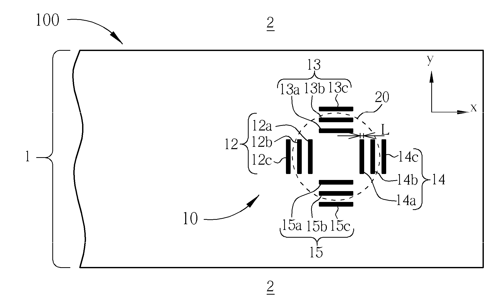
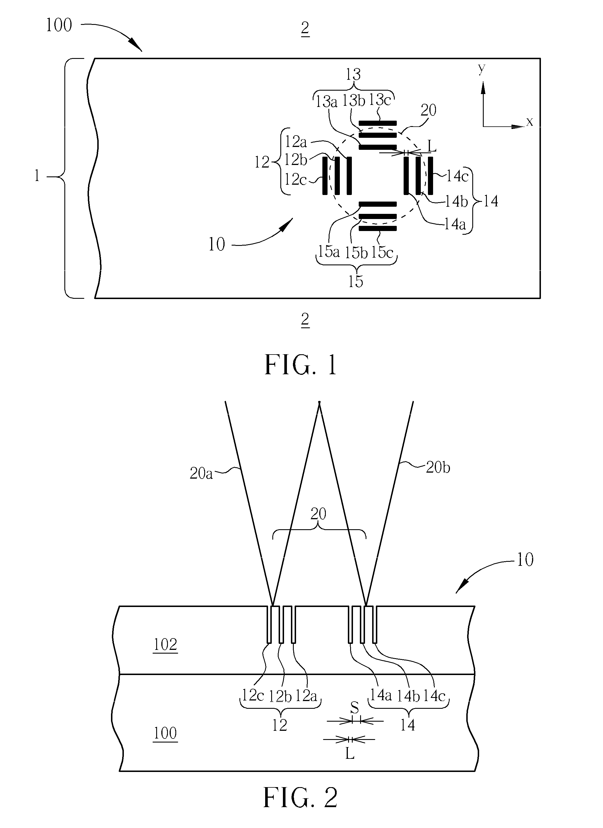
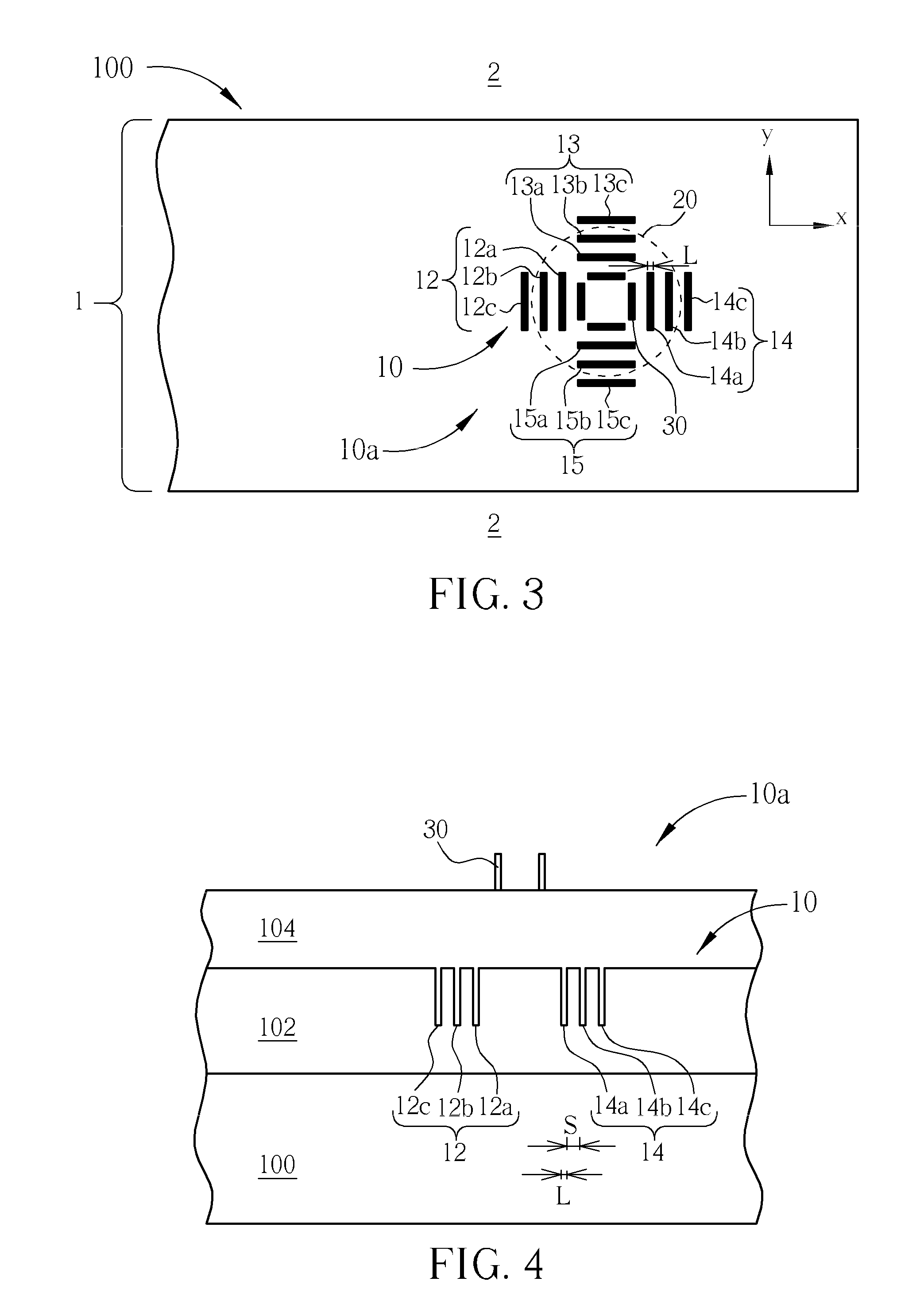
[0021]FIG. 1 is a schematic top view showing an enlarged portion of a scribe line on a semiconductor wafer according to one embodiment...


PUM


Abstract

An integrated alignment and overlay mark includes a pre-layer pattern for reticle-to-wafer registration implemented in an exposure tool, and a current-layer pattern incorporated with the pre-layer pattern. The pre-layer pattern and the current-layer pattern constitute an overlay mark for determining registration accuracy between two patterned layers on a semiconductor wafer.

Description

BACKGROUND OF THE INVENTION[0001]1. Field of the Invention[0002]The present invention relates generally to the manufacture of semiconductor wafers. More specifically, the present invention relates to an integrated alignment and overlay pattern for determining the registration accuracy between two patterned layers on a semiconductor wafer.[0003]2. Description of the Prior Art[0004]As known in the art, lithographic process is an essential step that determines the feature critical dimension (CD) in the manufacture of semiconductor integrated circuit device. Ordinarily, electric circuit patterns are formed by first transferring the pattern on a photo mask to a photoresist layer in a lithographic process, and then transferring the pattern from the photoresist layer to an underlying material layer such as a dielectric layer or a metal layer in a subsequent etching process.[0005]In order to increase production yield, alignment and overlay marks are typically provided on a wafer. By way of ...

Claims


Application Information

Patent Timeline
Patent Type & Authority Applications(United States)
IPC IPC(8): H01L23/544
CPCG03F7/70633G03F9/7084G03F9/7076G03F7/70683
Inventor CHIU, CHUI-FU
Owner NAN YA TECH
Why Eureka
Try Eureka